
FPGA design engineer and blogger, placing particular emphasis on test and formal verification
Gisselquist Technology, LLC,
Joined January 2017
- Tweets7.8K
- Following238
- Followers8.8K
- Likes8.5K






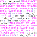
I needed to make certain the IP wasn't in one of the two states listed. The proper boolean expression would've required &&, not ||. As written with ||, the condition will always pass--the FSM state can never equal both of the states its being checked against at once.
Just for context, r_transfer is the name of the state variable -- although the bug would still be a bug either way.

Further, because this is intended to be an ASIC design, all cache accesses--both tag and memory--will be single port only, for area reduction purposes.
That's just a sample of some sticky details.
One subtle reality, is that the two streams (read/write) of such a cache cannot be independent. If nothing else, they will need arbitration to access tag memory. This is in contrast to most of my AXI work, where I try to keep the read/write FSMs as independent as possible.
This stack exchange post has a good description of the problems with using AES-CTR for memory encryption. I love the included pictures. They tell the story well.
crypto.stackexchange.com/que…
ROMs take space, but they can be placed on ASICs. It depends on your technology. ROMs that are small enough can be built out of logic. Yes, you can reset an internal RAM from a ROM. You can also use an external flash if necessary.
Three examples where memory reset is needed: 1) Security applications, where you have to guarantee no memory leakage, 2) Histogram accumulators, 3) GPS correlation accumulators. These aren't common examples, but they do happen.
It takes work--often a small FSM, coupled with a controller that holds READY low while running.
I had to do this with my histogram generator.
Sure, I get it.
There is one other issue to be aware of: If you get rid of the all internal reset, in favor of an initial statement, then the only way to reset the design will be a full reconfiguring of the FPGA. That's a design choice. Is it what you want?
Practically, that's what I used to do. I argued for it often. Then I came across issues with hardware that required resets. (The CPU hit a bug and needs to be reset, but I don't want to reset the whole system, the I2C system locked up, etc.) Resets within the design, even partial ones, can be quite valuable.
In the end, I just had to swallow my pride, say, "Yes, sir! That's a good catch. I'll fix it right away," and then go on with generating a new release.
Yes, I knew the first release would've worked, but no one wanted to take that chance on simple trust.
Arguably, the impact of any initial statements within a design on tainting any simulation results is a very real and valid threat to verifying any would-be ASIC IP, so I get their point.
It is frustrating to build and sell an IP to an ASIC customer, only to have the customer come back with, "See! We found a bug! You used an initial statement!" -- even if the initial statement, when dropped from the design, would have no impact.
One of the differences between ASIC and FPGA design is the initial statement. ASICs don't support them. To build IP that works across technologies, I've had to be very careful where, when, and how I use such statements. In many cases, I've had to remove them over time when my FPGA designs later become ASIC designs.

Here's the kicker. In one ASIC project, I was trying to cross from the JTAG clock domain to the system clock and back again. The two domains had separate and independent resets. To be useful, I had to AND the two negative edge resets together, then synchronize their release to get the CDC module to meet its formal assumptions.
Crossing reset domains like that breaks timing. I could no longer guarantee setup and hold timing on any of two individual reset paths, I could only accept the violation, accept that it would yield uncertain results for a clock cycle or two, and then go on. It's not ideal, and the hand-waiving stinks.
If you can think of a better solution, let me know and I'll try it.
I love the technique. I use it often. It's become a go-to approach for moving everything across clock domains slowly. As a result, the logic quietly moves from one project to another. It's now been in a couple ASIC projects as well.
Here's the post for reference:
zipcpu.com/blog/2020/10/03/t…
Some time ago, I posted an article on how to move values and strobes across clock domains. The module was powerful, very versatile, and easy to work with.
It had one flaw: it required a reset that would active in both clock domains at the same time, then synchronously release.
One of the challenges I've had with longer resets is that system reset control tends to be at the top level. Hence, when using a longer reset, you can no longer verify low level modules independently. (i.e., you have to assume the longer reset.)
So ... this can work ... for some IPs.
In this case, you'd need to make sure the input to the 2FF was reset, and then that the longer reset lasted at least 2 clocks in each domain--perhaps longer.