




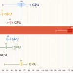


Bottleneck on Vera and Venice is less on per core performance than system bandwidth. Vera NVLink is the real advantage. Microbenches per core don't tell the full story where nowadays AMD and Nvidia sell compute racks, not CPUs.

AMD has followed up its Advancing AI data release with a new blog and a white paper on EPYC Venice that attempts to put real detail behind the claims first made on stage in July. The 2.24x platform and 1.2x per-core advantages over NVIDIA Vera in SPECrate 2026 Integer now come with estimated scores, compiler versions, memory configurations, and all 14 subtests broken out.
The generational data is impressive, with the 256-core EPYC 9996 landing between roughly 1.5x and 1.8x over the 192-core Turin flagship across Redis, NGINX, MySQL, MongoDB, and server-side Java, all measured by AMD on Venice silicon.
@AMD also rebuilt its 100 kW rack model around SPEC CPU 2026, which moved Venice to 3.4x over Vera and nudged its own Turin figure down slightly.
The core story is the same one AMD told at Advancing AI, now with some supporting detail. The agents-per-watt and performance-per-watt claims from the keynote have no backing data in this paper, interestingly. All of it is AMD internal testing or estimates, so independent results on shipping systems from both vendors are what will settle the debate.
Blog: newsroom.amd.com/news/amd-ep…
White paper: amd.com/content/dam/amd/en/d…


For those at the back of the room, Mehdi said that OpenAI didn’t solve the famous “can fluids explode by themselves?” puzzle. They added a fake extra shove and paid 10000 AIs millions of mucho dollars to fill out the paperwork. That’s not genius. That’s just cheating with a very expensive calculator and calling it a moon landing.

go fuck yourself @sama
claiming that you solved navier stokes because 10000 agents ran in circles for 88hours on a multimillion dollar gpu cluster to formalize in lean a blowup case under controlled external forcing is pure scientific vulgarity the clay mathematics institute millennium prize does not ask m whether you can artificially force a singularity in a fluid by injecting an ad hoc smooth external forcing term f(x,t) to twist the vortex until it breaks the real problem questions the fundamental stability and global smooth existence for 3dimensional incompressible euler & navier stokes equations under natural conservation laws and viscous dissipation alone using a mathematical loophole on forced equations to parade a century old victory is a major conceptual scam Altman
technically & epistemologically what you present as an agi breakthrough is nothing more than bruteforce combinatorial autoformalization the ai did not understand fluid mechanics it simply navigated a continuous search space previously mapped out and constrained by the monumental work of human mathematicians like tristan buckmaster/ levent alpöge / diego córdoba or tarek elgindi coordinating 10000 agents to check the logical consistency of a 100 page proof via lean is a software engineering feat and computational parallelization triumph not an intrinsic scientific discovery it is the victory of the compute bulldozer over abstract human intuition repackaged for the public as a higher mathematical consciousness
to this theoretical imposture you add a disgusting ethical and industrial cynicism taking advantage of private codex sessions and informal preprints from academic researchers to siphon their research leads and then trying to redact or erase the contribution of levent alpöge under the pretext that he works at rival anthropic is intellectual serfdom openai behaves like a feudal lord of silicon appropriating the cognitive subsistence of independent scholars threatening their careers behind closed doors if they protest and turning community academic labor into a privatized pressrelease
this entire staged event serves a desperate financial agenda in a pre ipo panic facing the slowdown of scaling laws and growing investor skepticism over the profitability of foundational models openai needs to manufacture an artificial sputnik moment claiming to solve a millennium prize without immediately submitting the proof to traditional peer review means using the prestige of fundamental mathematics as cheap marketing fuel to inflate a delusional valuation!!!
real science is not a clout chase on social media or a compute spike spent to rob the clay mathematics institute it is a quest for elegance physical truth and universal rigor to decode reality true artificial intelligence will not emerge from hostile corporate takeover of academic work hidden behind computational bruteforce but from architectures capable of generating new conceptual paradigms by masquerading constrained formalization as the collapse of physics greatest mysteries you did not solve navier stokes you only proved how far silicon valley will go to prostitute scientific integrity for capitalist spectacle

Good luck to Anthropic. For training, the cluster is the chip: Nvidia call it AI factory. You need CPU + GPU/XPU/TPU + scale-up/out network, everything as one memory domain. Starting now, they must match 2028 Nvidia Feynman: die stacking + NVHBM + NVLink CPO. Success odds: 0.1%


Poor analysis based on outdated usage. Local LLMs are so 2022. The real battle now is cluster scale agentic AI where each agent is launching 5-20 inferences and Vera Rubin is already 30 times faster than GB300. That's why OpenAI is buying more Nvidia than ever


It has been Nvidia game for a while:
Market predicts $102B
Nvidia estimates $108B
Nvidia delivers $115B
Rince and repeat

If Nvidia, $NVDA, actually reports $108 billion in revenue for Q3 as they are guiding, that would mark +1,730% growth in 4 years.
Never in history has a company of this size grown at such a fast pace.
Once again, we are witnessing history.
In a growing market, the game is not anymore on chip design and production at scale but also on procurement. Nvidia supply chain commitment jumped from $119B to $279B in one single quarter, mostly to secure more memory. In fact NVHBM for Feynman is already locked
Typical Samsung out of touch propaganda. Number on PowerPoint. Single digit real world yields, even years after introducing a new tech. Cough GAA cough
Samsung to Adopt 'Fork Sheet' for 1nm Process… All-Out Effort to Win Over Big Tech
Samsung Electronics' foundry division has set a target to introduce 1nm (nanometer; 1nm = one-billionth of a meter) process technology by 2031. The 1nm node is dubbed a "dream semiconductor" process, in which computing elements the width of just five atoms are arranged using an entirely new method. The goal is to engage in a head-to-head technology race with rival TSMC and seize leadership in the next-generation semiconductor market. Samsung is also developing a variety of process variants at its current cutting-edge 2nm node to secure major customers.
Fork Sheet Adoption… Aiming for a Fine-Pitch Process Breakthrough
According to industry sources on March 30, Samsung's foundry division plans to complete R&D on a 1nm semiconductor process by 2030 and transfer it to mass-production lines. The 1nm node is regarded as a dream-level innovation: it implies that the width of transistors—the elements responsible for data processing inside a chip—can shrink to just 1nm. Because that is half the transistor width of Samsung's current cutting-edge 2nm technology, process complexity rises significantly.
Alongside transistor scaling, the 1nm node will also introduce a new architecture called the "fork sheet." Up through the 2nm node, transistors have been built using Gate-All-Around (GAA) technology, which maximizes power efficiency by wrapping the gate around the channel on all four sides instead of three. The fork sheet takes this further by minimizing the spacing between GAA transistors. The technique inserts a non-conducting wall between GAA devices—much like driving a fork between them. Think of it this way: in a conventional layout, houses in a village are separated by open lawns; with fork sheet, those lawns are replaced by massive concrete walls. Just as removing the lawns frees up space to build more houses, fork sheet allows more transistors to be packed into the same chip area.
Chasing No. 1 TSMC
Samsung's foundry division ranks second globally, trailing TSMC—which commands nearly 70% market share—by roughly a factor of ten. TSMC, despite its dominant position, is also known to be pursuing fork-sheet adoption for its own 1nm-class process beyond 2030. Industry observers see Samsung's decision to lay out a 1nm roadmap targeting 2030 as a signal that it is preparing to compete with TSMC on equal technological footing.
Since announcing its "No. 1 in System Semiconductors by 2030" vision in 2019, Samsung has maintained a strategy of matching TSMC on leading-edge nodes. It was the first in the world to introduce extreme ultraviolet (EUV) lithography at the 7nm node in 2019, and the first to adopt GAA transistors at the 3nm node in 2022. An industry official noted: "It is realistically difficult for Samsung to overtake TSMC in revenue or production scale, but it continues to compete on the technology front. A prime example is last year's $16.5 billion (approximately KRW 25 trillion) contract with Tesla to supply 2nm AI chips—a milestone built on technological capability."
Rapid Diversification at the 2nm Node as Well
Samsung's foundry division is also rolling out multiple enhanced variants of its current cutting-edge 2nm technology. It is developing a custom process called "SF2T" for mass production of Tesla's 2nm AI chip, "AI6." Production of this chip will begin in 2027 at Samsung's new foundry hub in Taylor, Texas.
The division is also accelerating development of "SF2P," a new 2nm process to be deployed starting this year for manufacturing the next-generation smartphone application processor (AP) from Samsung's System LSI business, as well as "SF2P+," slated for activation next year. A semiconductor industry source said: "With 2nm process yields now exceeding 60% at peak, productivity has improved, and expectations for a return to profitability this year are growing."
So much for the naysayers, datacenters in space are a reality that can't be ignored anymore. And @elonmusk will be the winner. Exciting times

🚨 NVIDIA JUST ANNOUNCED DATA CENTERS IN SPACE
Jensen Huang:
>we’re going into space
>we’ve already been out in space
>announces “Vera Rubin Space-1”
>"in space there's no conduction, no convection, just radiation"
>"we have to figure out how to cool these systems in space"
>"we've got lots of great engineers working on it"
GPUs IN SPACE INCOMING
As I said last month when I called BS the fake new Korean media, Micron is part of Rubin HBM4 platform.

JENSEN TO MICRON CEO: To my friends at Micron. Our partnership changed the world. Industry’s fastest HBM4 delivered to NVIDIA.
Seems like Micron HBM4 is a go.
$MU $NVDA @MicronTech @NVIDIAGTC

Groq journey at Nvidia:
LP30 is a quick last minute addition.
LP35 blends into Nvidia software ecosystem (NVFP4).
LP40 adds Nvidia interconnect (NVLink).
LP-Next will co-packaged on-die.


That's simply a series of x86 CPUs with NVLink Fusion

BREAKING: $INTC Intel Announces they will be at $NVDA Nvidia GTC 2026, next week, March 16 - 19th.
Rumors suggest Intel will be releasing their new chips with Nvidia on x86 architecture.
For data centers:
Intel will build Nvidia-custom x86 CPUs that Nvidia will integrate into its AI infrastructure platforms and offer to the market.
For personal computing:
Intel will build and offer to the market x86 system-on-chips (SOCs) that integrate Nvidia RTX GPU chiplets. These new x86 RTX SOCs will power a wide range of PCs that demand integration of world-class CPUs and GPUs.
The custom x86 CPUs are specifically tailored for Nvidia’s AI platforms, enabling tight integration with NVLink for hyperscale / enterprise AI systems.

N3 capacity was set when Nvidia wasn't targeting top nodes & was smaller TSMC client than Apple.
It changes with Feynman: Nvidia is lead customer for A16 node, booking all early capacity like Apple once did.

Called it
@dylan522p just dropped the numbers: NVIDIA owns 70% of TSMC N3.
Google Cloud and DeepMind can’t agree on how many TPUs to give Anthropic.
Hard to be generous with chips you can’t guarantee for yourself.
One CEO controls delivery. That’s where the power sits. $nvda
Totally wrong. Nvidia Quantum-X Photonics InfiniBand switches like the Q3450-LD (144 ports at 800 Gb/s, 115 Tb/s aggregate) are already shipping NOW as we talk to CoreWeave, Lambda, and Texas Advanced Computing Center (TACC) with estimated sales of ~25k CPO switches in 2026.

Just brutal for the optical bulls. THIS IS EXACTLY WHAT the CEO of Credo told me Monday. CPO is not close. It is years away.
Broadcom CEO Hock Tan: “The best way .. is to use direct attached cooper. That’s the lowest latency, lowest power, and lowest cost .. you really want to use direct attached copper as long as you can .. All I’m trying to say is you don’t need to go run into some bright shiny objects called CPO [co-packaged optics]. Even as we are the leader in CPO. CPO will come in its time. Not this year. Maybe not next year. But in its time.”
Micron new 256GB LPDDR5X SOCAMM2 modules enable Vera Rubin systems to ship with up to 2TB of system RAM per CPU starting H2 2026.
This directly addresses the exploding demand for massive KV caches in long-context/agentic AI, thanks to coherent memory sharing via NVLink-C2C + low-latency Dynamo access. $MU $NVDA
bit.ly/Micron-256GB-SOCAMM2

Anthropic Downfall Scenario (post-supply-chain-risk ban):
- AWS, Google Cloud & Azure dump them fast to protect DoD billions
- Claude training stalls, enterprise clients flee to Grok/Gemini/GPT
- Valuation crashes from $380B → <$50B, IPO dead
Massive layoffs, cash burn
- 2027 fire sale: xAI buys for $20B, guts "woke" safeguards, absorbs talent/IP
Principles vs. power—power wins 🤷♂️

Anthropic is now "Supply-Chain Risk to National Security", meaning that companies working with them will also be excluded from gov contracts. It affects AWS, Azure, Google and dozens of other partners. That's huge and it will reshape the AI landscape
xitter.cf/SecWar/status/20275077…

This week, Anthropic delivered a master class in arrogance and betrayal as well as a textbook case of how not to do business with the United States Government or the Pentagon.
Our position has never wavered and will never waver: the Department of War must have full, unrestricted access to Anthropic’s models for every LAWFUL purpose in defense of the Republic.
Instead, @AnthropicAI and its CEO @DarioAmodei, have chosen duplicity. Cloaked in the sanctimonious rhetoric of “effective altruism,” they have attempted to strong-arm the United States military into submission - a cowardly act of corporate virtue-signaling that places Silicon Valley ideology above American lives.
The Terms of Service of Anthropic’s defective altruism will never outweigh the safety, the readiness, or the lives of American troops on the battlefield.
Their true objective is unmistakable: to seize veto power over the operational decisions of the United States military. That is unacceptable.
As President Trump stated on Truth Social, the Commander-in-Chief and the American people alone will determine the destiny of our armed forces, not unelected tech executives.
Anthropic’s stance is fundamentally incompatible with American principles. Their relationship with the United States Armed Forces and the Federal Government has therefore been permanently altered.
In conjunction with the President's directive for the Federal Government to cease all use of Anthropic's technology, I am directing the Department of War to designate Anthropic a Supply-Chain Risk to National Security. Effective immediately, no contractor, supplier, or partner that does business with the United States military may conduct any commercial activity with Anthropic. Anthropic will continue to provide the Department of War its services for a period of no more than six months to allow for a seamless transition to a better and more patriotic service.
America’s warfighters will never be held hostage by the ideological whims of Big Tech. This decision is final.
This:
Samsung Electronics is reportedly set to become the de facto exclusive supplier of 6th-generation High Bandwidth Memory (HBM4) for NVIDIA's top-tier AI GPU, "Vera Rubin,"
also:
SK Hynix currently has the most stabilized 1b DRAM production capacity, and accordingly, it is expected to maintain a relatively higher market share in the HBM4 market as well.
Conclusion: garbage article. Don't listen
Samsung Likely to Be Exclusive HBM4 Supplier for NVIDIA's Next-Gen Top-Tier GPU
Samsung Electronics is reportedly set to become the de facto exclusive supplier of 6th-generation High Bandwidth Memory (HBM4) for NVIDIA's top-tier AI GPU, "Vera Rubin," which is slated for full-scale launch in the second half of this year.
NVIDIA has been collaborating behind the scenes with Samsung Electronics on "Vera Rubin NVL72," its ultra-high-performance model, to achieve higher performance levels. Samsung's HBM4, which adopts more advanced process nodes than its competitors, has reportedly succeeded in maximizing performance, effectively securing a dominant position in the high-end product segment.
According to industry sources on February 20, NVIDIA plans to segment its HBM4 suppliers for next-generation GPUs into two categories: a general-purpose lineup prioritizing "stability" and a performance-oriented lineup targeting AI infrastructure requiring peak performance. While the general-purpose models are expected to account for the larger share of total supply volume, the estimated pricing of high-end products is projected to be 2–3x that of the previous generation, making them significantly more attractive from a profitability standpoint.
Samsung Electronics reportedly targeted the top-tier, highest-performance product segment from the early stages of HBM4 development, and its mass-produced HBM4 products have exceeded NVIDIA's specifications, creating clear differentiation from competitors. Unlike SK Hynix and Micron, which opted for 1b-nm (5th-generation 10nm-class) DRAM, Samsung preemptively adopted 1c-nm (6th-generation 10nm-class) DRAM. As DRAM process nodes continue to shrink, not only does chip productivity improve, but inherent performance and power efficiency also increase — directly impacting HBM4's maximum performance.
HBM, which is architected by stacking high-performance DRAM dies, is inherently sensitive to the performance of the underlying DRAM itself. Consequently, DRAM power efficiency and operating speed are the most critical variables determining HBM's peak performance. As DRAM scaling progresses to finer geometries, density, power efficiency, and productivity all improve. DRAM based on the 1c process node is known to deliver 10–20% better power efficiency and over 10% higher operating speeds compared to the previous generation. Samsung's HBM4 achieving a maximum speed of 13 Gbps — exceeding the international standard (JEDEC) by over 40% — is largely attributed to the adoption of the 1c process.
That said, the share of NVIDIA's high-end GPUs within the total AI semiconductor market remains uncertain. This will depend on the CAPEX direction of hyperscalers including OpenAI, Google, Meta, Microsoft, and Amazon. If hyperscaler investment turns conservative, general-purpose models could dominate the market over high-end GPU demand.
SK Hynix, for its part, appears focused on supply stability rather than outright performance. Its overwhelming dominance in the HBM market serves as a key advantage, and its partnership with NVIDIA remains firmly intact. SK Hynix currently has the most stabilized 1b DRAM production capacity, and accordingly, it is expected to maintain a relatively higher market share in the HBM4 market as well.
However, industry consensus is that time is on Samsung Electronics' side. As the HBM market increasingly levels up and becomes a "weight class battle," Samsung's production capacity and market influence are expected to stand out. A source with close knowledge of Samsung noted: "The most critical variable for next-generation HBM is the stability and performance of the underlying DRAM. If Samsung's 1c DRAM yields reach maturity, it could send another shockwave through the market."
