





If this is the forecast for AMD, think what happens when Intel comes out with Jaguar Shores!

$AMD Morgan Stanley has cut SUBSTANTIALLY its demand estimates on AMD GPU units, reflecting a potentially fundamental shift in AI compute demand dynamics.
Wondering how they developed such dramatic forecasting model. This kind of cut should be based on comprehensive check from all sources, including supply chain. I would expect AMD to make a strong statement soon countering Morgan Stanley’s claim.


TSMC: “We have no intention of leaving any food on the table for others.”
Meanwhile…
KeyBanc: “Intel Foundry wins with Apple are expected to be on 14A…”
😂😂😂
Thank god! Based on some reports, I was really worried that some high-end Nova Lake desktop tiles might end up on 18A-P. But that’s not the case.
All high end desktop tiles are on N2P. And that’s the way it should be for higher clocks and better thermals.
18A-P is best suited for laptop, mobile, server & ai parts. Not for high power, high frequency, high thermal desktop parts.


Wow! Sydney Sweeney as Cortana!!

🆕️JUST IN: Sydney Sweeney is reportedly going to play Cortana in Denis Villeneuve adaptation of Halo which will be the first project for the new entertainment division for #XBOX.

Intel 14A & Elon's Terafab:
"You don’t become a Trillionaire by throwing away money!"
I’ll say it again:
Intel sharing 14A tech (and beyond) with Terafab is never good for Intel. When the news first came out, I was very worried. Now I’m happy it didn’t go through.
Simply put, Elon is one of the best there is when it comes to making deals. He’s that good. And once Terafab is fully operational and it doesn’t need Intel anymore, Intel will naturally get the royal shaft. Elon is that ruthless.
You don’t become a Trillionaire by throwing away money!
Thank god Intel didn’t go for the deal. 14A & beyond solely belongs to Intel and that’s the way it should be!
Share your thoughts…
Image credit: TechPowerUp

Gotta give it to my $INTC fam, yall really held it down after the Great Elon Betrayal of 2026. Market really said Elon/Terrafab don’t matter (yet).
LETS GO 🔥
Gr8 news! Intel Nova Lake with big fucking cache (BFC) is launching earlier that expected!
a.k.a bLLC

SemiAnalysis on Intel 18A Density: A real banger!?
"Our measurements put Panther Lake’s 18A compute logic and TSMC N3E GPU logic at similar logic density. However, 18A does not lead TSMC N3P, N2 or Samsung SF2 in peak density."
First, Panther Lake CPU tile uses Intel 18A HP library. Whereas, Panther Lake iGPU uses the 2-2 HD library. Their statement comparing 18A & N3E is incorrect cos one is HP & the other is HD.
Second, they don't use Cell Utilization when comparing FSPDN/BSPDN nodes. Again, that's incorrect.
Lunar Lake CPU tile is 105 mm2 (without iGPU). Whereas, PTL-U 338H (4+0+4) CPU tile is only 91 mm2 (without iGPU). This is in spite of PTL-U 338H having extra 4MB L2 + 6 MB L3 cache. This size difference between the LNL & PTL CPU Tile is around 15%. If we remove this extra 10MB of cache from PTL-U and compare apples to apples, the difference is around 20%.
How is 18A able to pack more in significantly less area?
This is because of 18A higher "Cell Utilization". This puts 18A clearly ahead of *all* 3nm class nodes. 18A is close to N2 & 18A-P is closer to N2P.
The key purpose of BSPDN is to move the power rails, metals, grid, bumps to the backside, freeing up area in the front side. This freed up area in the frontside can accommodate more logic/sram. In a theoretical 100 mm2 pure FSPDN logic die (like TSMC N2P), only up to 75 mm2 can be used for pure logic. Whereas, in a theoretical 100 mm2 pure BSPDN logic die (like Intel 18A-P), over 90 mm2 can be used for pure logic according to Intel. This gives BSPDN nodes like 18A a solid edge in overall logic density. (Note: All density comparisons are theoretical peaks and not to be taken literally.)
So, w.r.t to my previous post, comparing densities of a FSPDN nodes like N2/N3 with a BSPDN nodes like 18A/18A-P without using Cell Utilization is a big mistake. Guaranteed to give wrong results.
Image Source: Semi Analysis
Link: newsletter.semianalysis.com/…
(For more details, see my previous post on this.)
Share your thoughts. Follow/Repost if you like. 👍

Riddle me this: 18A vs N3E
If we make the exact same die on Intel 18A and TSMC N3E, why on earth is the N3E die bigger by 20% ?
Yes. 20% bigger!!!
Like I said, 18A is a “2nm”’class node and not to be compared with any 3nm class process nodes.
More info:
SemiAnalysis on Intel 18A Density: A real banger!?
"Our measurements put Panther Lake’s 18A compute logic and TSMC N3E GPU logic at similar logic density. However, 18A does not lead TSMC N3P, N2 or Samsung SF2 in peak density."
First, Panther Lake CPU tile uses Intel 18A HP library. Whereas, Panther Lake iGPU uses the 2-2 HD library. Their statement comparing 18A & N3E is incorrect cos one is HP & the other is HD.
Second, they don't use Cell Utilization when comparing FSPDN/BSPDN nodes. Again, that's incorrect.
Lunar Lake CPU tile is 105 mm2 (without iGPU). Whereas, PTL-U 338H (4+0+4) CPU tile is only 91 mm2 (without iGPU). This is in spite of PTL-U 338H having extra 4MB L2 + 6 MB L3 cache. This size difference between the LNL & PTL CPU Tile is around 15%. If we remove this extra 10MB of cache from PTL-U and compare apples to apples, the difference is around 20%.
How is 18A able to pack more in significantly less area?
This is because of 18A higher "Cell Utilization". This puts 18A clearly ahead of *all* 3nm class nodes. 18A is close to N2 & 18A-P is closer to N2P.
The key purpose of BSPDN is to move the power rails, metals, grid, bumps to the backside, freeing up area in the front side. This freed up area in the frontside can accommodate more logic/sram. In a theoretical 100 mm2 pure FSPDN logic die (like TSMC N2P), only up to 75 mm2 can be used for pure logic. Whereas, in a theoretical 100 mm2 pure BSPDN logic die (like Intel 18A-P), over 90 mm2 can be used for pure logic according to Intel. This gives BSPDN nodes like 18A a solid edge in overall logic density. (Note: All density comparisons are theoretical peaks and not to be taken literally.)
So, w.r.t to my previous post, comparing densities of a FSPDN nodes like N2/N3 with a BSPDN nodes like 18A/18A-P without using Cell Utilization is a big mistake. Guaranteed to give wrong results.
Image Source: Semi Analysis
Link: newsletter.semianalysis.com/…
(For more details, see my previous post on this.)
Share your thoughts. Follow/Repost if you like. 👍
Intel 18A vs TSMC N2P: 18A Kicks Ass!
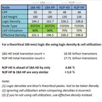
We now have standard cell library metrics of N2P and 18A directly from Synopsys. Below is the chart that shows the logic densities and cell utilization of both N2P & 18A. Synopsys metrics attached below for reference.
In HD, density difference between N2P & 18A is only around 6.8%.
In HP, they're the same!
In SRAM, they're the same! (38.1Mb/mm2)
18A-P is a performance enhanced version of 18A, does not improve density. Both 18A & 18A-P are design rule compatible. Similarly, N2P is a performance enhanced version of original N2, does not improve density. Both N2 & N2P are design rule compatible.
When comparing logic densities of FSPDN & BSPDN process nodes, ignoring cell utilization is literally wrong, cos it gives completely wrong results. Simple reason is, FSPDN nodes (like TSMC N2P) have low cell utilization (lower than 75%) compared to BSPDN nodes (like Intel 18A) which have very high cell utilization (greater than 90%). If you're not using cell utilization when comparing densities, use effective densities instead.
FSPDN nodes (like N2P) have a solid advantage when it comes to high frequency designs like Zen 6 & Nova Lake. The heat can easily dissipate directly thru the TIM/IHS. Whereas, BSPDN nodes (like 18A) have some hotspot issues cos the heat has to dissipate thru additional metal layer and then thru the TIM/IHS. This additional layer reduces Fmax by a bit. But by how much exactly is still unknown, cos we never had a high frequency desktop design on 18A coupled with a large heat sink. My guess is, 18A Fmax penalty is probably around ~10% compared to N2 variants.
In essence, 18A is Intel's first true "2nm class" node.
Share your thoughts. Follow/Repost if you like. 👍


If you're wondering why Intel Nova Lake high-end high-frequency desktop CPUs are on TSMC N2P and not on 18A-P, the reason is simple:
FSPDN nodes (like N2P) have a solid advantage when to comes to high frequency designs like Zen 6 & Nova Lake. The heat can easily dissipate directly thru the TIM/IHS. Whereas, BSPDN nodes (like 18A) have some hotspot issues cos the heat has to dissipate thru additional metal layer and then thru the TIM/IHS. This additional layer reduces Fmax by a bit. But by how much exactly is still unknown, cos we never had a high frequency desktop design on 18A coupled with a large heat sink. My guess is, 18A Fmax penalty is around ~10% compared to N2 variants.
That's the reason Nova Lake high-end high-frequency SKUs are on N2P.
If NVL high-end desktop CPUs end up on 18A-P and has lower turbo frequency than Zen 6 top-end SKUs, I'd say, it's one of the worst decision Intel has ever made. I'm sincerely hoping NVL top-end 18A-P rumors are false.
Intel 18A vs TSMC N2P: 18A Kicks Ass!
We now have standard cell library metrics of N2P and 18A directly from Synopsys. Below is the chart that shows the logic densities and cell utilization of both N2P & 18A. Synopsys metrics attached below for reference.
In HD, density difference between N2P & 18A is only around 6.8%.
In HP, they're the same!
In SRAM, they're the same! (38.1Mb/mm2)
18A-P is a performance enhanced version of 18A, does not improve density. Both 18A & 18A-P are design rule compatible. Similarly, N2P is a performance enhanced version of original N2, does not improve density. Both N2 & N2P are design rule compatible.
When comparing logic densities of FSPDN & BSPDN process nodes, ignoring cell utilization is literally wrong, cos it gives completely wrong results. Simple reason is, FSPDN nodes (like TSMC N2P) have low cell utilization (lower than 75%) compared to BSPDN nodes (like Intel 18A) which have very high cell utilization (greater than 90%). If you're not using cell utilization when comparing densities, use effective densities instead.
FSPDN nodes (like N2P) have a solid advantage when it comes to high frequency designs like Zen 6 & Nova Lake. The heat can easily dissipate directly thru the TIM/IHS. Whereas, BSPDN nodes (like 18A) have some hotspot issues cos the heat has to dissipate thru additional metal layer and then thru the TIM/IHS. This additional layer reduces Fmax by a bit. But by how much exactly is still unknown, cos we never had a high frequency desktop design on 18A coupled with a large heat sink. My guess is, 18A Fmax penalty is probably around ~10% compared to N2 variants.
In essence, 18A is Intel's first true "2nm class" node.
Share your thoughts. Follow/Repost if you like. 👍

This means the world’s first 1.4nm chip Intel Razor Lake RZL-UL built on Intel 14A is coming out next year end as planned in limited volume. TSMC A14 comes a year later.

Intel's 14A process will begin trial production ahead of schedule in Q1 next year.
$INTC
Like i said before, this means NVL might easily match or surpass apple m5 silicon in both st & mt. But might trail behind m6. That’s the cost of backward compatibility.
X86S can fix that to an extend, but it may not get adopted anytime soon, as it slightly reduce backward compatibility of existing 32 bit apps which are still widely used today.
