

That's the power of Intel inside.
Joined October 2023
- Tweets2.3K
- Following249
- Followers2.2K
- Likes5.7K








The Inteller retweeted
What does it really take to make the world's most advanced chips?
Thousands of intricate manufacturing steps. Extraordinary engineering precision. And an industry working to meet growing global demand for computing.
Get an inside look at Intel's semiconductor innovation as Chris Auth, Pushkar Ranade, and other Intel experts join @dwarkeshpodcast to explore the science, technology, and manufacturing expertise behind advanced chips.
Watch the full conversation: ms.spr.ly/6014aaFMm
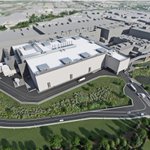
Intel Ohio Fab 27 just hit a major construction milestone: the first truss in place, which marks a significant step toward the high volume production for Intel 14A external customers.
Back in 2022, Fab 52's first truss was set in December. Tool installation was underway in H2 2024, and the fab completed its 1st wafer in Q1 2025, roughly 9 quarters after the "first truss" milestone.
If Ohio Fab 27 follows a similar timeline or even accelerates the build-out, tool move-in in early 2028 and HVM in late 2028 could be achievable. That's well ahead of the official 2030 operational target.
Meanwhile, tool installation at Arizona Fab 62 is already underway, with operations expected by 2028.
Combined with Ireland Fab 34's capacity expansion and the Fab 38 wildcard in Israel, 2028 could mark a major turning point in Intel's global manufacturing footprint.

Building semiconductor leadership requires innovation and the manufacturing capacity to bring it to scale.
In a new piece, Naga Chandrasekaran shares how Intel Foundry is expanding that capacity across the U.S., including progress on our Ohio site, where the initial major structural truss has been installed on first fab.
Read more: ms.spr.ly/6015aauoh
The Inteller retweeted

Foveros 2.5D enables high-density interconnects and heterogeneous chiplet integration, giving designers flexibility to combine different dies, process nodes, and IP in a single package.
Learn more: ms.spr.ly/6016aSNIQ
#IntelFoundry
The Inteller retweeted

Former Intel CEO Pat Gelsinger on getting hired at 18, designing Intel's chips while finishing his PhD, and arguing with his Stanford professors:
"I'm 16 years old. I accidentally win a scholarship. I go to tech school, skip my last year and a half of high school, and Intel comes recruiting when I'm 18 years old."
"The interviewer, he writes on his page, and I was number 12 that he interviewed that day... He says, 'Smart, aggressive, arrogant. He'll fit right in.'"
"I was engineer number four on the 386. Architect and design manager for the 486. All of that while doing my bachelor's, my master's and PhD work... Learning by day, and putting it to practice at night."
"One of the professors postulated a new carry lookahead adder design in one of my classes at Stanford. So I said, 'Well, I'm working on the 386 carry lookahead adder, so let me go try it.'"
"I come back two days later to the professor and I said, 'It doesn't work.' The next two class periods were just me and the professor arguing over why his design didn't work."
@PGelsinger @RaghuRaghuram @appenz

Former Intel CEO Pat Gelsinger with a16z's Raghu Raghuram and Guido Appenzeller on the next wave of semiconductor innovation and the physical constraints shaping the AI buildout:
Drawing on his experience designing Intel's 386 and 486 processors, Pat explains how AI could transform chip design, but also why faster design alone won't solve the industry's biggest problems.
They examine the bottlenecks in manufacturing, memory bandwidth, advanced packaging, and power, and why today's explosion of specialized AI chips may eventually consolidate around a smaller number of architectures.
They also discuss the potential for new memory technologies, the shift from copper to optical networking, and why energy capacity could become a major constraint on AI growth.
Finally, they revisit Pat's VMware years to ask what virtualization might look like when infrastructure is built for agents rather than humans.
YouTube: youtu.be/1Q_7yU7FZ1k
1:05 Hired by Intel at 18
3:50 Arguing with Stanford professors
7:25 Will AI design the next gen chips?
8:45 Designing faster than fabs can build
11:55 Why GPUs are stuck with bad memory
13:40 Why 100 AI chips will collapse to a few
19:15 Agents make new chips cheap to run
22:10 No new memory chip since the 90s
27:20 Why 16-layer chip stacks are a fantasy
32:15 The physics that keeps memory next to compute
34:55 "I declared the death of copper"
38:05 AI traffic breaks the internet's design
42:40 "Energy capacity equals economic capacity"
46:25 The 130-year-old power war AI reopened
48:50 VMware for agents
@PGelsinger @RaghuRaghuram @appenz
The Inteller retweeted

Not an expert but to the best of my understanding
One chart changed how I think about EUV.
I used to think EUV was only about making smaller chips.
But another benefit is simpler manufacturing.
Without EUV:
Print → Clean → Print → Clean → Print → Clean
With EUV:
Print → Clean
You still need cleaning, but far fewer times.
Less steps, less mistakes
3nm doesn't have 10× more mistakes.
It has roughly 10× more chances to make a mistake.
Think about it like this:
65nm: 100 cleaning steps
3nm: 1000 cleaning steps
If each step has a tiny chance of error, then doing 10x more steps creates many more chances for something to go wrong.
One mistake. Game over for the chip.
That's why advanced chip manufacturing is so hard.
Source: Nomura ANCHOR REPORT
China semiconductor equipment and materials

This is why I’ve stayed quiet on the TeraFab–TSMC speculation.
I simply don’t see the mutual incentive.
TSMC is the process leader. Why hand out the crown jewels and potentially hurt its own foundry business?
Intel has the opposite incentive: licensing can strengthen customer confidence, while external capital can expand its manufacturing reach.
TSMC has the cash to build capacity itself. Intel has every reason to leverage other people’s capital.
The incentives just don’t line up.

I discussed the broader 14A / Fab strategy in my Substack here:
intelpromaxultra.substack.co…

2. Large-die yields remain a real challenge:
I think this is one of the hidden drawbacks of Intel’s current product mix.
On 18A, both Clearwater Forest and Diamond Rapids rely on relatively small compute dies. That is great for product architecture, but it is less helpful if you want to prove out large-die yield capability for hyperscaler ASIC customers.
In other words, Intel can ramp 18A successfully for its own small-chiplet server products and still remain less prepared for customers that need very large logic dies.
That is why I think Coral Rapids matters strategically.
If it embraces a larger-die design again, 14A could become a much more credible node for hyperscaler ASIC business — not just a strong internal CPU node.
More thoughts in the note:
1. The bar for foundry breakeven seems to be moving higher:
Previously, Intel suggested foundry breakeven could be achieved largely with internal volume plus a $3–5B annual run-rate basis external business.
But now the discussion involves 40K WPM of external client volume. Even if assuming a relatively cheap $15,000 ASP, that already implies about $7.2B revenue for wafer business only.
And once you add EMIB-T’s “multi-billion-dollar” packaging business, the implied external foundry scale can very easily move above $10B.
So to me, Intel increasingly seems to be targeting a much larger external foundry business before calling the model “breakeven.”
Naga’s latest comments on 14A closely align with the framework I laid out back in my August Substack article.
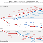
I estimated Intel 14A to be 1.68x and TSMC A14 to be 1.75x, which implies 14A would trail A14 by only ~4% in perf. (Naga: Within ~5% to A14).
More broadly, my model also places 18A/A-P (1.43x~1.56x) between TSMC N3 and N2P (1.38x~1.63x), which also aligns with Naga's claim in the interview.


Naga Chandrasekaran who is the EVP, CTO, and GM, Intel Foundry. In a meeting with Keybanc told them:
Intel, "Expects 14A performance to be within 5% of TSM's A14".
Intel is not afraid of CoPoS. "Sees sustained leadership in
advanced packaging with EMIB-T even with TSM introducing CoPoS".
I must say that the news around 14A PPA is truly extraordinary given 14A yields and ramp are extremely aggressive. Intel is finally sticking its neck out to say how their nodes compare with a % range to TSMC.
Note goes on to say that Intel has a server part on 14A in 2028. Coral Rapids might not be on 18A-U if that's the case. Coral could be 14A, but I have capacity concerns (2029 is the big ramp, pointings towards 2029 Ohio volume)
$INTC

Under Intel’s own push toward concentrating HVM in 1–2 major sites, that makes a dedicated third 14A geography in Israel less compelling.
But that does not make Fab 38 less valuable. It can remain Intel’s manufacturing wildcard:
intelpromaxultra.substack.co…

Oregon still has another expansion lever: D1X Module 4.
Intel has already secured development approval for the future module, giving the campus another major block of advanced-node capacity when needed.
Combine that with:
• Existing D1X modules (M1, M2, M3)
• Older fab space that can be repurposed (D1B, D1C, D1D)
• >1M sq. ft. of cleanroom
• Brownfield retrofit potential
• Future Module 4 expansion
and Oregon already looks like an HVM-scale manufacturing campus, even while preserving substantial space for technology development.
I also find Intel’s increasing use of the “Fab 25” designation interesting. The naming fits a broader transition in Oregon’s role, from primarily a TD complex toward a formal part of Intel’s HVM network.
The distinction between “development fab” and “production fab” is becoming much less rigid.

Intel is undergoing a paradigm shift in how it allocates fab capacity. Historically, Oregon played the role of the technology-development hub to develop the process → early ramp → transfer HVM elsewhere.
For 14A, that model is changing.
Intel now wants Oregon to participate in high-volume manufacturing. Physically, that makes much more sense than it may sound.
Oregon campus already has >1M sq. ft. of cleanroom space, with a substantial portion capable of supporting EUV-based process flows.
As older processes roll off, Intel can reuse that footprint through the same playbook we are now seeing in Ireland: cleanroom retrofit + process-flow splitting + old tool reuse / new tooling.
Oregon is no longer just where Intel invents the next node, it is becoming a place where Intel can manufacture it at scale.

The management publicly announced that 0.2 is around the corner for 14A, and you tell me 18A only got 0.2?