
Documenting the journey from $0 to infinity. Options, mindset, discipline.
Joined December 2025
- Tweets767
- Following19
- Followers134
- Likes465






Zero to Infinity retweeted
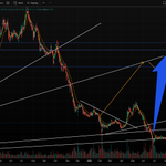
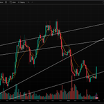
Macro moves the markets. It kind of paves the ground for the major trends.
If only you could position ahead. However, staying nimble is as important.
Zero to Infinity retweeted

Flydubai captain Smit Machchhar: “I knew these might be my final moments, I was ready to die. But I told myself: just open the door, just do it.”
One of the greatest heroes in history 🙏🇮🇳🇮🇱
Zero to Infinity retweeted
$SNOW could hit $400 soon. Here's why: Snowflake has quickly transformed from a cloud-native company into a "cloud agent-native" one. This has a direct impact on billing and revenue, since unit token consumption is increasing as more customers use Snowflake's data products.
This shift is already happening, but I expect it to accelerate — tokens are expensive, and the longer and more complex the context, the more expensive the final output token from the LLM.
So I expect Snowflake's revenue to grow significantly — potentially from $1.25B to $5B, with a PE of ~17. I'm expecting revenue to roughly 3x over the next 3 years, with a long curve tilted toward the upside. Token economics will improve over time, but token generation and consumption will keep scaling regardless.
Targeting $780 before Dec 2027.
Zero to Infinity retweeted
If the BTC move is real, it can rally to 101K. $MSTR rallied 280% in two months last time this happened. OOM calls went nuts — 50x to 150x.

Zero to Infinity retweeted
$ASML — my 1100 and 1700 targets hit way early (was expecting Dec 2026). Added it to my watchlist in Sept 2025 at 770; that's a $1200 move in 10 months. The 1200C 12/18/26 I added to my watchlist then is up 30X.
This is that time again. Nothing wrong with ASML — but they can only grow 13-19% annually. They're capped by their own supply chain and talent: 60 machines now, ~80 by 2027. Not enough to justify this multiple.
I think this is the top, or it could stretch to 3000.


Zero to Infinity retweeted

One of the most iconic images in American history
U.S. Marines raising the American flag on Mount Suribachi during the Battle of Iwo Jima — February 23, 1945
A symbol of courage, sacrifice, and the unbreakable American will to win
Freedom was never handed down
It was fought for


Zero to Infinity retweeted

SUMMARY OF FED CHAIR WARSH'S STATEMENT:
1. Shorter Fed policy statement is intended to "give you the facts"
2. Forward guidance in Fed statement "not well-suited" to current policy state
3. Establishes new "independent task forces" in 5 key areas
4. Task forces will propose next steps including changes to the Summary of Economic Projections
5. The Fed will be maintaining its 2% inflation objective
6. Fed policy appears to be restrictive for housing, but not financial markets
A new era of Fed policy is ahead of us.
Zero to Infinity retweeted
SUMMARY OF FED DECISION (6/17/2026):
1. Fed leaves rates unchanged for the 4th straight meeting
2. 9 out of 18 officials expect at least one rate hike this year
3. Fed lowers its median 2026 US GDP projection from 2.4% to 2.2%
4. Fed now sees PCE inflation not returning to its 2% target until 2028
5. Fed says inflation "remains elevated" relative to their goal
6. Today's Fed decision was reached in a unanimous 12-0 vote
The Fed appears to be bracing for more inflation.



Zero to Infinity retweeted

Samsung Electronics: The Last Piece in Normalizing Its Semiconductor Business Is ‘Packaging’
Samsung Electronics’ semiconductor business has moved into a full rebound led by high bandwidth memory (HBM) and foundry. In advanced packaging, however, which has emerged as a core of AI chip manufacturing, the company has yet to establish a clear presence. The industry view is that securing major customers in 2.5D packaging, in particular, is urgent.
According to industry sources on the 8th, cumulative shipments of Samsung Electronics’ in house 2.5D packaging technology ‘Cube’ are understood to still be small. The orders secured so far are also said to consist largely of startup initial volumes or short term, project based work. This stands in contrast to major competitors TSMC and Intel, which are aggressively expanding their 2.5D packaging businesses.
TSMC and Intel Surge Ahead… Samsung Electronics Lacks Major 2.5D Packaging Customers
2.5D packaging is a technology that inserts a thin film interposer between the semiconductor chip and the substrate to boost chip performance. Its importance is growing steadily in the semiconductor industry. This is because AI accelerators, an essential element of AI data centers, are made by integrating high performance system semiconductors and HBM through 2.5D packaging. Indeed, during the period when the HBM market was expanding, Samsung Electronics wielded as a weapon a business model offering its foundry, HBM, and 2.5D packaging on a turnkey basis.
In packaging, Samsung Electronics has worked since 2024 to expand the market for its in house 2.5D packaging technology Cube. However, there is no confirmed case yet of Samsung Electronics’ 2.5D packaging being adopted in a big tech AI accelerator. The customers currently using Samsung Electronics’ 2.5D packaging are understood to include IBM of the US and Rebellions, a domestic AI fabless startup.
One industry official in packaging explained, “Customers that have adopted Samsung Electronics’ 2.5D packaging platform remain at low shipment volumes or short term, project based production on a monthly cycle,” adding, “Now that we have entered an era in which advanced packaging significantly determines chip performance, Samsung Electronics also needs to concentrate on reinforcing its competitiveness in this field.”
This contrasts with Samsung Electronics’ main competitors TSMC and Intel, each of which is achieving remarkable growth in 2.5D packaging.
TSMC, which leads the global foundry market, is executing investments to expand the production capacity of its in house 2.5D packaging ‘Chip on Wafer on Substrate (CoWoS)’ from around 35,000 wafers per month at the end of last year to around 130,000 wafers per month by the end of this year.
Intel is moving into full commercialization of its 2.5D packaging ‘Embedded Multi die Interconnect Bridge (EMIB).’ Google is reported to have adopted EMIB for mass production of its own AI chip, the Tensor Processing Unit (TPU), and is expected to begin mass production from next year.
Larger Chips… Samsung Electronics Sees a Possible Turnaround with PLP
It is not as though Samsung Electronics has no opportunities. The company is currently shifting the development direction of its 2.5D packaging from the existing wafer level packaging (WLP) to panel level packaging (PLP).
Panel level packaging is a process that performs packaging on a wide rectangular panel. Compared with packaging on the existing wafer (300mm in diameter), it offers a larger area and allows chips to be arranged efficiently, resulting in higher productivity. In particular, with recent AI semiconductors growing in chip size to improve performance, the applicability of PLP is expected to expand.
Accordingly, Samsung Electronics is applying PLP instead of WLP to Cube, while also pursuing commercialization of ‘System on Panel (SoP)’ for ultra large chips. SoP is a technology that joins multiple semiconductors together on a large rectangular panel, and is currently being developed at a size of 415x510mm.
Another industry official in packaging stated, “Samsung Electronics’ neglect of mass production development for advanced packaging technology for system semiconductors, relative to memory semiconductors, risks acting as a factor that undermines its future business competitiveness,” and noted, “At the point when PLP application begins in earnest in the AI chip field, it will need to quickly secure I-Cube customers.”
Meanwhile, setting aside 2.5D packaging, Samsung Electronics’ semiconductor business is showing a clear overall improvement this year. Aggressive AI infrastructure investment by global big tech has greatly increased demand for advanced semiconductors, and the development of advanced processes has also picked up speed.
In February, Samsung Electronics began mass production shipments of HBM4 (the 7th generation of HBM) for NVIDIA, laying the cornerstone for a rebound in its sluggish HBM business. The company has also set a plan to expand HBM shipments by more than three times year over year this year. There are expectations that the foundry business will turn to profit as early as the second half of this year. It has recently attracted Tesla, NVIDIA, and Groq, among others, as advanced process customers.

Zero to Infinity retweeted
I can say that Mizuho’s numbers are not irrational at all — they are actually quite reasonable.
Access Citrini’s institutional report here: citrini.com/contact

Zero to Infinity retweeted
[Exclusive] Samsung Foundry Expected to Return to Profit in Q3 This Year… "Entering Growth Trajectory After Four Years"
Observations are emerging internally that Samsung Electronics' foundry division could succeed in turning a profit as early as the third quarter of this year. Analysts point to improved production volumes of advanced 2nm process nodes and the base die used in high bandwidth memory (HBM) as factors giving momentum to profitability improvement.
According to the industry on the 8th, the timing of the breakeven target that Samsung Electronics' foundry division had set is expected to be moved up to the third quarter of this year, from the originally projected end of this year through next year, on the back of yield improvements and the effect of large order wins. This would mark an earnings recovery roughly four years after the trillion won scale operating losses that began in 2022. There is an assessment that the foundry division, long identified as the Achilles heel of Samsung's semiconductor business, has entered a structural improvement trajectory faster than expected.
First, Samsung Electronics' advanced process is performing better than expected. Samsung Electronics is reported to have raised the yield of its 2nm GAA (gate all around) process to over 60% as of the first quarter of this year. While it still falls short of the 70% level regarded as the benchmark for mass production economics, the industry assesses this as a sufficient level to carry out initial volume production while simultaneously securing new customers. In its first quarter 2026 earnings announcement in April, Samsung Electronics said that "utilization of its advanced process lines has reached maximum levels." Despite the seasonal off peak period, it is understood to have achieved double digit revenue growth compared to the same period a year earlier.
In addition, the customer acquisition activity that has continued since last year is set to convert into full scale revenue in the second half. Samsung Electronics signed a 22.8 trillion won long term supply contract for autonomous driving chips with Tesla in July last year, and plans to begin 2nm mass production of AI5 and AI6 chips at its Taylor plant in Texas, USA, starting in the second half of this year. NVIDIA CEO Jensen Huang also publicly certified Samsung Electronics' contract manufacturing when he unveiled the AI inference dedicated chip "Grok3" during his keynote at "GTC 2026" in March.
The scale of orders is also growing rapidly. Samsung Electronics internally projects that the number of 2nm related orders this year will increase by more than 130% compared to the previous year, and beyond Tesla and NVIDIA, it is expanding the scope of cooperation with multiple big tech firms including Apple and Nintendo. There are also reports that the volume of sixth generation HBM (HBM4) base die has already reached a sold out level.
Cost soundness is also expected to improve as mass production ramp up at the Taylor fab soon reverses the fixed cost structure. The Taylor fab, into which 37 billion dollars (about 54 trillion won) was invested, had been a factor deepening the foundry division's losses by generating enormous construction costs. An official familiar with Samsung Electronics explained that "once mass production gets into full swing in the second half, the calculation shows that the depreciation burden could instead turn into a fixed cost dilution effect, sharply improving the profit and loss structure."
The fact that the advanced process lines of competitor TSMC of Taiwan have effectively entered a saturated state due to a surge in demand for AI accelerators is also working in Samsung Electronics' favor. Some fabless (semiconductor design) firms are actively considering Samsung Electronics as an alternative, and there are observations that AMD is reviewing a dual foundry strategy for a portion of its next generation graphics processing unit (GPU) volumes.

Zero to Infinity retweeted

3D DRAM will unlock a whole new dimension (literally) in computer architecture.
It'll be presented at ISCA 2026 later this month.
3 things you should know:
1. Stacking DRAM on compute, allows us to co-design them together just like how it is done with SRAM now.
2. The power numbers are very good 0.3-0.4 pJ/bit (compared to HBM's 3-4 pJ/bit).
3. 3D dram allows you to pull 100K+ lanes into the compute die, unlike 2K lanes in HBM4. Imagine the speed.
I co-authored this paper. It'll be part of the conference proceedings, but I'll write an article on chiplog.io shortly after.

Zero to Infinity retweeted
Container shipping rates are surging amid the Iran War:
The spot rate for a 40-foot container from Asia to the US West Coast jumped +$655, or +20%, over the last week, to ~$3,933, the highest in at least 6 months.
At the same time, the rate from Asia to Northern Europe jumped +$793, or +27%, to ~$3,649.
Since the start of the Iran War, Asia-to-US container rates have surged +109%, and Asia-to-Europe rates are up by more than +50%.
This comes as shipments rerouted around the blocked Strait of Hormuz are causing severe congestion at Southeast Asian transshipment hubs, including Singapore and Malaysia.
On top of this, carriers are charging importers fuel surcharges and shifting costs, while a pickup in demand heading into peak season for booking ocean freight is adding further pressure.
Looking ahead, available shipping capacity is set to shrink further as importers rush to replenish inventories in July and August, which could push rates even higher.
Supply chain pressures are intensifying.

Zero to Infinity retweeted

Iran's new missile strikes on Israel raise a larger question:
What if the Iran War is entering a new phase?
For 35 years, the world believed overwhelming military superiority guaranteed political control.
The Iran War is forcing us to reconsider that assumption.
On Prof Pape Substack, my new essay:
The World After Iran