

Park Systems is a world-leading manufacturer of nanometrology tools for surface analysis in research and industry.
Joined November 2011
- Tweets4.2K
- Following1.1K
- Followers7.9K
- Likes368




Resolving 2D materials means capturing more than one length scale at once. In the image below, 𝗣𝗮𝗿𝗸 𝗡𝗫𝟭 reveals twisted bilayer graphene on SiC with both the atomic honeycomb lattice and the longer-period moiré superlattice visible in the same dataset.
The moiré pattern shows a periodicity of ~1.5 nm, superimposed on the graphene lattice with its characteristic 2.46 Å interatomic spacing. The FFT confirms both signals simultaneously: inner spots from the moiré periodicity and outer hexagonal spots from the atomic lattice.
For researchers studying twist angle, stacking order, and van der Waals heterostructures, 𝗡𝗫𝟭 𝗯𝗿𝗶𝗻𝗴𝘀 𝗮𝘁𝗼𝗺𝗶𝗰 𝗮𝗻𝗱 𝗺𝗼𝗶𝗿é 𝗶𝗺𝗮𝗴𝗶𝗻𝗴 𝗶𝗻𝘁𝗼 𝗮 𝘀𝘁𝗮𝗯𝗹𝗲, 𝗽𝗿𝗮𝗰𝘁𝗶𝗰𝗮𝗹 𝗔𝗙𝗠 𝘄𝗼𝗿𝗸𝗳𝗹𝗼𝘄.
💡𝗘𝘅𝗽𝗹𝗼𝗿𝗲 𝗣𝗮𝗿𝗸 𝗡𝗫𝟭: okt.to/pPaCJG
Image caption: LFM imaging of twisted bilayer graphene on SiC with Park NX1: (a,b,e) atomic lattice + moiré pattern, (c) FFT, (d) graphene lattice.
#AFM #Graphene #2DMaterials #Moiré #Nanotechnology #ParkSystems

How does automation expand what is possible in advanced 2D materials research?
In our new 𝗰𝘂𝘀𝘁𝗼𝗺𝗲𝗿 𝗰𝗮𝘀𝗲 𝘀𝘁𝘂𝗱𝘆, 𝗥𝗲𝗯𝗲𝗰𝗮 𝗥𝗶𝗯𝗲𝗶𝗿𝗼-𝗣𝗮𝗹𝗮𝘂 of Université Paris-Saclay shares how 𝗣𝗮𝗿𝗸 𝗙𝗫𝟰𝟬 𝘀𝗶𝗺𝗽𝗹𝗶𝗳𝗶𝗲𝘀 𝗱𝗲𝗺𝗮𝗻𝗱𝗶𝗻𝗴 𝗔𝗙𝗠 𝘄𝗼𝗿𝗸𝗳𝗹𝗼𝘄𝘀 in a busy multi-user lab. Automated probe exchange, reliable mode switching, and precise return to the same region help make complex measurements more reproducible across users.
The case study also highlights how FX40 enables precise mechanical manipulation of sophisticated 2D devices, as demonstrated in controlled angular studies of dynamically rotatable bilayer graphene/hBN heterostructures, recently published in 𝗡𝗮𝘁𝘂𝗿𝗲 𝗠𝗮𝘁𝗲𝗿𝗶𝗮𝗹𝘀 (DOI: 10.1038/s41563-026-02667-7).
👉 𝗥𝗲𝗮𝗱 𝘁𝗵𝗲 𝗰𝗮𝘀𝗲 𝘀𝘁𝘂𝗱𝘆 𝗮𝗻𝗱 𝗲𝘅𝗽𝗹𝗼𝗿𝗲 𝗣𝗮𝗿𝗸 𝗙𝗫𝟰𝟬: okt.to/TvzINj
#ParkSystems #FX40 #AFM #2DMaterials #Graphene #hBN #Nanotechnology
Image caption: Park FX40 AFM error-signal images show a dynamically rotatable bilayer graphene/hBN heterostructure at two angular configurations. The hBN rotator was mechanically manipulated with the AFM tip in contact mode to control the relative layer alignment. Images courtesy of Université Paris-Saclay and CNRS.

𝗛𝗼𝘄 𝗰𝗮𝗻 𝘆𝗼𝘂 𝘀𝘁𝘂𝗱𝘆 𝗯𝗮𝘁𝘁𝗲𝗿𝘆 𝗶𝗻𝘁𝗲𝗿𝗳𝗮𝗰𝗲𝘀 𝘄𝗵𝗶𝗹𝗲 𝗲𝗹𝗲𝗰𝘁𝗿𝗼𝗰𝗵𝗲𝗺𝗶𝗰𝗮𝗹 𝗽𝗿𝗼𝗰𝗲𝘀𝘀𝗲𝘀 𝗮𝗿𝗲 𝗮𝗰𝘁𝘂𝗮𝗹𝗹𝘆 𝗵𝗮𝗽𝗽𝗲𝗻𝗶𝗻𝗴?
Discover how SECCM, conductive AFM, electrochemical AFM and PinPoint™ nanomechanical mapping provide complementary information on battery electrodes. The webinar will show how these methods probe solid-electrolyte interphase formation, local nanomechanical properties and real-time volume changes at the nanoscale during operation.
🎤𝗦𝗽𝗲𝗮𝗸𝗲𝗿: Prof. Prof. Dr. @Christine Kranz, Ulm University, Germany
👉𝗥𝗲𝗴𝗶𝘀𝘁𝗲𝗿: okt.to/KhNjUf
#SECCM #AFM #Electrochemistry #BatteryMaterials #Nanotechnology

At SEMICON West? Meet Park Systems at Booth #245!
Explore in-line AFM metrology for precise wafer measurements and 3D surface characterization, supporting evolving needs in AI and advanced packaging.
📍 Moscone Center, San Francisco | Oct 13–15
#SEMICONWest #ParkSystems


Conductive AFM on 2D materials faces a demanding challenge: resolving local electrical contrast while preserving atomic-scale structural information in the same scan.
This image of Bernal-stacked bilayer graphene on silicon carbide, acquired on the 𝗣𝗮𝗿𝗸 𝗡𝗫𝟭, shows how much detail conductive AFM can reveal.
𝗧𝘄𝗼 𝗳𝗲𝗮𝘁𝘂𝗿𝗲𝘀 𝘀𝘁𝗮𝗻𝗱 𝗼𝘂𝘁:
🔹 Atomic lattice: the top graphene layer shows its hexagonal lattice, with a pitch of about 2.5 Å.
🔹 Moiré pattern: a superstructure with ~1.8 nm periodicity, arising from the lattice mismatch between the carbon buffer layer and the SiC substrate.
The measurement was performed on Park NX1 with a Femto DLPCA-200 current amplifier and using a PPP-EFM probe from @NANOSENSORS.
💡𝗘𝘅𝗽𝗹𝗼𝗿𝗲 𝗺𝗼𝗿𝗲 𝗮𝗯𝗼𝘂𝘁 𝗡𝗫𝟭: okt.to/XbIYmc
Sample courtesy of Prof. @Martin Rejhon, Institute of Physics, Charles University, Prague. Thank you for kindly providing the sample!
#AFM #Graphene #2DMaterials #Nanotechnology #ConductiveAFM #ParkSystems #MaterialsScience

Women shape the future of science.
This 𝗔𝗱𝗮 𝗟𝗼𝘃𝗲𝗹𝗮𝗰𝗲 𝗗𝗮𝘆, Park Systems celebrates women advancing semiconductors, materials and energy research, and affirms equal rights, recognition and opportunities across STEM.
Who inspires your work?
#AdaLovelaceDay #WomenInSTEM

Final Call | PFM Webinar 🔬
Explore PFM fundamentals and advanced techniques including Contact-Resonance PFM and DFRT-PFM for nanoscale characterization of piezoelectric and ferroelectric materials.
📅 October 13, 2026
🔗 Register now: okt.to/39BugV
#AFM #PFM #MaterialsScience

[Press Release] Park Systems 𝗹𝗲𝗮𝗱𝘀 𝘁𝗵𝗲 𝗴𝗹𝗼𝗯𝗮𝗹 𝗔𝗙𝗠 𝗺𝗮𝗿𝗸𝗲𝘁 by revenue for the fourth consecutive year (2022–2025), according to QY Research AFM Market Report. With 23.8% of global AFM revenue and 340 systems sold in 2025, the company ranked first in revenue and unit shipments.
Building on this leadership, Park Systems has expanded its research-grade AFM portfolio with 𝗡𝗫𝟭 𝗳𝗼𝗿 𝗮𝘁𝗼𝗺𝗶𝗰-𝘀𝗰𝗮𝗹𝗲 𝗶𝗺𝗮𝗴𝗶𝗻𝗴 under ambient conditions, while broadening its capabilities through 𝗶𝗺𝗮𝗴𝗶𝗻𝗴 𝘀𝗽𝗲𝗰𝘁𝗿𝗼𝘀𝗰𝗼𝗽𝗶𝗰 𝗲𝗹𝗹𝗶𝗽𝘀𝗼𝗺𝗲𝘁𝗿𝘆 (𝗜𝗦𝗘) and 𝗱𝗶𝗴𝗶𝘁𝗮𝗹 𝗵𝗼𝗹𝗼𝗴𝗿𝗮𝗽𝗵𝗶𝗰 𝗺𝗶𝗰𝗿𝗼𝘀𝗰𝗼𝗽𝘆 (𝗗𝗛𝗠).
These developments come as the global AFM market is forecast to grow from $508.69 million in 2025 to $1.01 billion by 2032, at a compound annual growth rate of 11.23%.
💡𝗥𝗲𝗮𝗱 𝘁𝗵𝗲 𝗳𝘂𝗹𝗹 𝗽𝗿𝗲𝘀𝘀 𝗿𝗲𝗹𝗲𝗮𝘀𝗲: okt.to/9Zpweg
#ParkSystems #AFM #Nanometrology #AFMleader

They did it again! 💪🏃
Another year, another 𝗚ö𝘁𝘁𝗶𝗻𝗴𝗲𝗻 𝗢𝗯𝘀𝘁𝗮𝗰𝗹𝗲 𝗖𝗶𝘁𝘆 𝗥𝘂𝗻 for the 𝗣𝗮𝗿𝗸 𝗦𝘆𝘀𝘁𝗲𝗺𝘀 𝗔𝗰𝗰𝘂𝗿𝗶𝗼𝗻 𝘁𝗲𝗮𝗺. This time, 18 colleagues faced 6 km and 21 obstacles, pushing through nearly three hours of running, climbing, crawling, water, mud and plenty of teamwork.
A tough challenge, a strong team and one more finish line crossed together. Congratulations to everyone who took part and brought the Park Systems team spirit to the course! 🎉
Already wondering what challenge comes next... 😎
#ParkSystems #TeamSpirit #ObstacleCityRun #Göttingen


One technique rarely answers every question in a complex sample.
𝗔𝘁𝗼𝗺𝗶𝗰 𝗙𝗼𝗿𝗰𝗲 𝗠𝗶𝗰𝗿𝗼𝘀𝗰𝗼𝗽𝘆, 𝗡𝗮𝗻𝗼-𝗜𝗥 𝘀𝗽𝗲𝗰𝘁𝗿𝗼𝘀𝗰𝗼𝗽𝘆, 𝗜𝗺𝗮𝗴𝗶𝗻𝗴 𝗦𝗽𝗲𝗰𝘁𝗿𝗼𝘀𝗰𝗼𝗽𝗶𝗰 𝗘𝗹𝗹𝗶𝗽𝘀𝗼𝗺𝗲𝘁𝗿𝘆 and 𝗗𝗶𝗴𝗶𝘁𝗮𝗹 𝗛𝗼𝗹𝗼𝗴𝗿𝗮𝗽𝗵𝗶𝗰 𝗠𝗶𝗰𝗿𝗼𝘀𝗰𝗼𝗽𝘆 reveal complementary information: from structure and chemistry to thin-film properties and dynamics.
🔔Follow Park Systems for multimodal measurement ideas you can apply in the lab.
The @CAS International Semiconductor Conference, IEEE event brings together researchers and engineers working across semiconductor devices, micro- and nanosystems, MEMS, sensors and advanced materials.
We are also pleased to contribute to the scientific program with a plenary presentation by 𝗗𝗿. 𝗝𝗮𝗺𝗲𝘀 𝗞𝗲𝗿𝗳𝗼𝗼𝘁, Park Systems UK Ltd.:
"𝗔𝘁𝗼𝗺𝗶𝗰 𝗙𝗼𝗿𝗰𝗲 𝗠𝗶𝗰𝗿𝗼𝘀𝗰𝗼𝗽𝘆 𝗳𝗼𝗿 𝗡𝗮𝗻𝗼𝘀𝗰𝗮𝗹𝗲 𝗠𝗼𝗿𝗽𝗵𝗼𝗹𝗼𝗴𝗶𝗰𝗮𝗹 𝗮𝗻𝗱 𝗘𝗹𝗲𝗰𝘁𝗿𝗶𝗰𝗮𝗹 𝗖𝗵𝗮𝗿𝗮𝗰𝘁𝗲𝗿𝗶𝘀𝗮𝘁𝗶𝗼𝗻 𝗼𝗳 𝗦𝗲𝗺𝗶𝗰𝗼𝗻𝗱𝘂𝗰𝘁𝗼𝗿𝘀"
Thursday, October 15 | 10:00 | Room 1
The talk will explore emerging AFM applications including ferroelectric and memristive devices, dopant and carrier mapping, buried-interface characterization, and nanoscale chemical analysis using nano-IR spectroscopy.
If you are attending CAS 2026, visit us and @Schaefer SEE Srl to discuss your semiconductor, MEMS and nanoscale characterization challenges.
💡𝗟𝗲𝗮𝗿𝗻 𝗺𝗼𝗿𝗲 𝗮𝗯𝗼𝘂𝘁 𝗣𝗮𝗿𝗸 𝗦𝘆𝘀𝘁𝗲𝗺𝘀 𝗦𝗼𝗹𝘂𝘁𝗶𝗼𝗻𝘀: okt.to/wTBxY6
#semiconductors #AFM #MEMS #nanotechnology #Metrology #DigitalHolographicMicroscopy #ParkSystems

Explore oxide thin films with ISE 🔬
Learn how Imaging Spectroscopic Ellipsometry enables high-resolution mapping of film thickness and optical properties while revealing local variations across oxide thin films.
📅 October 27, 2026
🔗 Register: okt.to/bzUWjJ
#ISE #ThinFilms #Metrology

What does fully automated AFM metrology look like? From wafer loading to analysis, 𝗣𝗮𝗿𝗸 𝗡𝗫-𝗪𝗮𝗳𝗲𝗿 𝗮𝘂𝘁𝗼𝗺𝗮𝘁𝗲𝘀 𝗲𝗮𝗰𝗵 𝗸𝗲𝘆 𝘀𝘁𝗲𝗽: receiving the host recipe, selecting the probe, aligning the wafer, moving to target sites, measuring and reporting.
Reduce manual intervention and bring repeatable nanoscale metrology into semiconductor production.
💡𝗦𝗲𝗲 𝘁𝗵𝗲 𝘄𝗼𝗿𝗸𝗳𝗹𝗼𝘄. 𝗟𝗲𝗮𝗿𝗻 𝗺𝗼𝗿𝗲: okt.to/QXbUgp
We were excited to meet so many researchers in Boston and see our tools in action at 𝗡𝗔𝗡𝗢𝘀𝗰𝗶𝗲𝗻𝘁𝗶𝗳𝗶𝗰 𝗦𝘆𝗺𝗽𝗼𝘀𝗶𝘂𝗺 𝗔𝗺𝗲𝗿𝗶𝗰𝗮𝘀 𝟮𝟬𝟮𝟲 this week.
Park Systems supported live demonstrations and hands-on sessions with advanced 𝗔𝗙𝗠, 𝗗𝗶𝗴𝗶𝘁𝗮𝗹 𝗛𝗼𝗹𝗼𝗴𝗿𝗮𝗽𝗵𝗶𝗰 𝗠𝗶𝗰𝗿𝗼𝘀𝗰𝗼𝗽𝘆, 𝗮𝗻𝗱 𝗜𝗺𝗮𝗴𝗶𝗻𝗴 𝗦𝗽𝗲𝗰𝘁𝗿𝗼𝘀𝗰𝗼𝗽𝗶𝗰 𝗘𝗹𝗹𝗶𝗽𝘀𝗼𝗺𝗲𝘁𝗿𝘆.
It was great to see participants testing workflows, asking detailed questions, and discussing real applications directly with our team.
We were also pleased to sponsor the 𝗕𝗲𝘀𝘁 𝗣𝗼𝘀𝘁𝗲𝗿 𝗔𝘄𝗮𝗿d and recognize outstanding research presented during the symposium.
#ParkSystems #NANOscientific Symposium #NSSAmericas #AFM #DHM #ISE #SPM #Nanoscience”


Explore PFM at the nanoscale 🔬
Learn the fundamentals of Piezoresponse Force Microscopy and explore advanced techniques including Contact-Resonance PFM and DFRT-PFM for piezoelectric and ferroelectric materials.
📅 October 13, 2026
🔗 Register: okt.to/No9tb3
#AFM #PFM #MaterialsScience

𝗛𝗼𝘄 𝘀𝗺𝗮𝗹𝗹 𝗮 𝘃𝗶𝗯𝗿𝗮𝘁𝗶𝗼𝗻 𝗰𝗮𝗻 𝗗𝗶𝗴𝗶𝘁𝗮𝗹 𝗛𝗼𝗹𝗼𝗴𝗿𝗮𝗽𝗵𝗶𝗰 𝗠𝗶𝗰𝗿𝗼𝘀𝗰𝗼𝗽𝘆 (𝗗𝗛𝗠) 𝗿𝗲𝗹𝗶𝗮𝗯𝗹𝘆 𝗺𝗲𝗮𝘀𝘂𝗿𝗲? In Journal of Physics: Photonics, authors address a key challenge in MEMS vibration mapping: separating real nanoscale motion from measurement noise. They define a rigorous way to determine the DHM detection limit, show how experimental settings affect it, and propose a metric for comparing systems.
To validate their approach, the researchers measured the vibration mode of a phononic crystal, an experiment requiring a 𝗱𝗲𝘁𝗲𝗰𝘁𝗶𝗼𝗻 𝗹𝗲𝘃𝗲𝗹 𝗼𝗳 𝗷𝘂𝘀𝘁 𝟭 𝗽𝗶𝗰𝗼𝗺𝗲𝘁𝗲𝗿. This resolution is 𝗳𝗿𝗲𝗾𝘂𝗲𝗻𝗰𝘆 𝗮𝗻𝗱 𝗺𝗲𝗮𝘀𝘂𝗿𝗲𝗺𝗲𝗻𝘁 𝗯𝗮𝗻𝗱𝘄𝗶𝗱𝘁𝗵 𝗶𝗻𝗱𝗲𝗽𝗲𝗻𝗱𝗲𝗻𝘁.
Because DHM 𝗰𝗮𝗽𝘁𝘂𝗿𝗲𝘀 𝘁𝗵𝗲 𝗲𝗻𝘁𝗶𝗿𝗲 𝗳𝗶𝗲𝗹𝗱 𝗼𝗳 𝘃𝗶𝗲𝘄 simultaneously, it reveals such small vibration patterns across the structure extremely rapidly, 𝘄𝗶𝘁𝗵𝗼𝘂𝘁 𝗽𝗼𝗶𝗻𝘁-𝗯𝘆-𝗽𝗼𝗶𝗻𝘁 𝘀𝗰𝗮𝗻𝗻𝗶𝗻𝗴
This approach can support more reliable characterization of 𝗠𝗘𝗠𝗦, 𝗺𝗶𝗰𝗿𝗼𝘀𝗲𝗻𝘀𝗼𝗿𝘀, 𝗿𝗲𝘀𝗼𝗻𝗮𝘁𝗼𝗿𝘀, 𝘂𝗹𝘁𝗿𝗮𝘀𝗼𝗻𝗶𝗰 𝗱𝗲𝘃𝗶𝗰𝗲𝘀 𝗮𝗻𝗱 𝗽𝗵𝗼𝗻𝗼𝗻𝗶𝗰 𝘀𝘁𝗿𝘂𝗰𝘁𝘂𝗿𝗲𝘀.
📜𝗥𝗲𝗮𝗱 𝘁𝗵𝗲 𝗳𝘂𝗹𝗹 𝗽𝗮𝗽𝗲𝗿: okt.to/oQuc8s
💡𝗘𝘅𝗽𝗹𝗼𝗿𝗲 𝗿𝗲𝗹𝗮𝘁𝗲𝗱 𝗗𝗛𝗠 𝗮𝗽𝗽𝗹𝗶𝗰𝗮𝘁𝗶𝗼𝗻𝘀: okt.to/ZMmcp3
Image caption: DHM vibration-amplitude map of a phononic crystal used to validate picometer-scale detection, with vibration at a resonance node measured down to 1.26 pm.
#DHM #MEMS #Photonics #Microscopy #Microsensors #Phononics

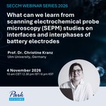
𝗪𝗵𝗮𝘁 𝗵𝗮𝗽𝗽𝗲𝗻𝘀 𝗮𝘁 𝗲𝗹𝗲𝗰𝘁𝗿𝗼𝗱𝗲 𝗶𝗻𝘁𝗲𝗿𝗳𝗮𝗰𝗲𝘀 𝗰𝗮𝗻 𝗱𝗲𝘁𝗲𝗿𝗺𝗶𝗻𝗲 𝗵𝗼𝘄 𝘁𝗵𝗲 𝗲𝗻𝘁𝗶𝗿𝗲 𝗯𝗮𝘁𝘁𝗲𝗿𝘆 𝗽𝗲𝗿𝗳𝗼𝗿𝗺𝘀.
In this webinar, explore how 𝘀𝗰𝗮𝗻𝗻𝗶𝗻𝗴 𝗲𝗹𝗲𝗰𝘁𝗿𝗼𝗰𝗵𝗲𝗺𝗶𝗰𝗮𝗹 𝗽𝗿𝗼𝗯𝗲 𝗺𝗶𝗰𝗿𝗼𝘀𝗰𝗼𝗽𝘆 (𝗦𝗘𝗣𝗠) techniques and 𝗔𝗙𝗠-𝗯𝗮𝘀𝗲𝗱 𝗺𝗲𝘁𝗵𝗼𝗱𝘀 reveal interfacial and interphase processes that are difficult to capture with alternative techniques. See how nanoscale measurements 𝗰𝗼𝗻𝗻𝗲𝗰𝘁 𝘀𝘂𝗿𝗳𝗮𝗰𝗲 𝗺𝗼𝗿𝗽𝗵𝗼𝗹𝗼𝗴𝘆, 𝗺𝗲𝗰𝗵𝗮𝗻𝗶𝗰𝗮𝗹 𝗽𝗿𝗼𝗽𝗲𝗿𝘁𝗶𝗲𝘀 𝗮𝗻𝗱 𝗲𝗹𝗲𝗰𝘁𝗿𝗼𝗰𝗵𝗲𝗺𝗶𝗰𝗮𝗹 𝗯𝗲𝗵𝗮𝘃𝗶𝗼𝗿 in emerging battery materials.
🎤𝗦𝗽𝗲𝗮𝗸𝗲𝗿: Prof. Prof. Dr. @Christine Kranz, Ulm University, Germany
👉𝗥𝗲𝗴𝗶𝘀𝘁𝗲𝗿 𝗻𝗼𝘄: okt.to/21neV6
#Electrochemistry #BatteryResearch #AFM #SECCM #EnergyStorage

Every reliable AFM measurement starts before the probe reaches the wafer. Park NX-Wafer 𝗮𝘂𝘁𝗼𝗺𝗮𝘁𝗲𝘀 𝘄𝗮𝗳𝗲𝗿 𝘁𝗿𝗮𝗻𝘀𝗳𝗲𝗿, 𝗮𝗹𝗶𝗴𝗻𝗺𝗲𝗻𝘁, 𝘁𝗮𝗿𝗴𝗲𝘁 𝗽𝗼𝘀𝗶𝘁𝗶𝗼𝗻𝗶𝗻𝗴 𝗮𝗻𝗱 𝗽𝗿𝗼𝗯𝗲 𝗲𝘅𝗰𝗵𝗮𝗻𝗴𝗲 for 300 mm workflows. Its EFEM supports precise handling, including warped wafers, while the tip exchanger stores up to 24 pre-mounted probes. See wafer handling designed for semiconductor fabs.
💡𝗟𝗲𝗮𝗿𝗻 𝗺𝗼𝗿𝗲: okt.to/50kdVi
[𝗡𝗮𝗻𝗼𝘀𝗰𝗮𝗹𝗲 𝗘𝗹𝗲𝗰𝘁𝗿𝗼𝗰𝗵𝗲𝗺𝗶𝘀𝘁𝗿𝘆: 𝗦𝗜𝗖𝗠 𝗪𝗲𝗲𝗸 / 𝗘𝗽𝗶𝘀𝗼𝗱𝗲 𝟱]
In this example, we use a Park NX20 AFM to perform complementary analysis of the top surface of a Norwegian maple leaf, first in air with conventional AFM and then in a PBS buffer with SICM.
The extreme aspect ratio of pulled glass nanopipettes used in SICM is beneficial when measuring rough surfaces such as leaves while 𝘁𝗵𝗲 𝘂𝘀𝗲 𝗼𝗳 𝗶𝗼𝗻 𝗰𝘂𝗿𝗿𝗲𝗻𝘁 𝗳𝗲𝗲𝗱𝗯𝗮𝗰𝗸 𝗲𝗻𝗮𝗯𝗹𝗲𝘀 𝗲𝘃𝗲𝗻 𝘃𝗲𝗿𝘆 𝘀𝗼𝗳𝘁 𝘀𝘂𝗿𝗳𝗮𝗰𝗲 𝗳𝗲𝗮𝘁𝘂𝗿𝗲𝘀 𝘁𝗼 𝗯𝗲 𝗰𝗵𝗮𝗿𝗮𝗰𝘁𝗲𝗿𝗶𝘇𝗲𝗱 𝗶𝗻 𝗹𝗶𝗾𝘂𝗶𝗱 𝗲𝗻𝘃𝗶𝗿𝗼𝗻𝗺𝗲𝗻𝘁𝘀.
💡𝗙𝗶𝗻𝗱 𝗼𝘂𝘁 𝗺𝗼𝗿𝗲 𝗮𝗯𝗼𝘂𝘁 𝗦𝗜𝗖𝗠 𝗵𝗲𝗿𝗲: okt.to/iPnyMI
#SICM #ScanningIonConductanceMicroscopy #BioImaging #Nanopipette #ScanningProbeMicroscopy #AFM okt.to/OIKbZt
[𝗡𝗮𝗻𝗼𝘀𝗰𝗮𝗹𝗲 𝗘𝗹𝗲𝗰𝘁𝗿𝗼𝗰𝗵𝗲𝗺𝗶𝘀𝘁𝗿𝘆: 𝗦𝗜𝗖𝗠 𝗪𝗲𝗲𝗸 / 𝗘𝗽𝗶𝘀𝗼𝗱𝗲 𝟰]
Scanning ion conductance microscopy (SICM) enables nanoscale imaging of samples under biologically relevant conditions without applying mechanical force, which is especially valuable for cells. Blood platelets change their morphology when activated and forces exerted during conventional AFM imaging can trigger this process artificially.
Using SICM on a Park Systems AFM, platelets can be 𝗶𝗺𝗮𝗴𝗲𝗱 𝗶𝗻 𝗮𝗻 𝗶𝘀𝗼𝘁𝗼𝗻𝗶𝗰 𝗲𝗻𝘃𝗶𝗿𝗼𝗻𝗺𝗲𝗻𝘁 𝗶𝗻 𝘁𝗵𝗲𝗶𝗿 𝗻𝗮𝘁𝗶𝘃𝗲, 𝘂𝗻𝗮𝗰𝘁𝗶𝘃𝗮𝘁𝗲𝗱 𝘀𝘁𝗮𝘁𝗲, 𝗲𝗻𝗮𝗯𝗹𝗶𝗻𝗴 𝘁𝗵𝗲𝗶𝗿 𝗮𝗰𝘁𝗶𝘃𝗮𝘁𝗶𝗼𝗻 𝘁𝗼 𝗯𝗲 𝘀𝘁𝘂𝗱𝗶𝗲𝗱 𝗶𝗻 𝘀𝗶𝘁𝘂.
💡𝗙𝗶𝗻𝗱 𝗼𝘂𝘁 𝗺𝗼𝗿𝗲 𝗮𝗯𝗼𝘂𝘁 𝗦𝗜𝗖𝗠 𝗶𝗺𝗮𝗴𝗶𝗻𝗴 𝗼𝗳 𝗯𝗶𝗼𝗹𝗼𝗴𝗶𝗰𝗮𝗹 𝗰𝗲𝗹𝗹𝘀 𝗵𝗲𝗿𝗲: okt.to/ecE4zT
#SICM #ScanningIonConductanceMicroscopy #LiveCellImaging #BioImaging #CellBiology #Platelets #ScanningProbeMicroscopy

