
manufacturing, supply chains, AI, DC buildout. Building weapons grade system for monitoring the situation.
Abu Dhabi
Joined March 2026
- Tweets243
- Following66
- Followers17
- Likes138





Pinned Tweet
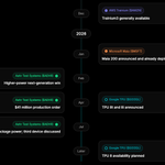
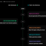
updated nvidia roadmap, courtesy of @0xBADB01E "big boss" - xitter.cf/0xBADB01E/status/20739…


So following these principles here is the architecture that falls out and it’s quite different than what is thought to be optimal today.
Starting with the memory: LPDDR6 tops out around 14.4 Gb/s per pin. We would want to as many channels as the die’s edge can carry. If we can fit 24 channels, that’s 576 data pins, and you get ~1 TB/s per chip with 192 GB of storage. Same as the b200 in size but about an a100 in bandwidth.
But remember that LPDDR access latency is ~100 ns which is about the same as HBM. So streaming weights from LPDDR costs you nothing on latency and we just give up per package bandwidth, and remember our pipelining already collapsed that requirement.
Now work backwards to compute. Tokens/sec = ~aggregate BW / bytes touched per token, and at batch 64 in FP4 every delivered byte wants ~256 FLOPs. 1 TB/s × 256 = ~260 TF of FP4. Size ~280 TF for some headroom and stop! That’s all we need, the rest of the alpha is in latency tuning not flops.
Now process node, again using first principles thinking. On TSMC N6 that MAC array would be about 30 mm^2. The rest of the die goes to SRAM buffers, 24 LPDDR PHYs, and 56 lanes of plain 32 GT/s NRZ SerDes PCIe 5.0 transceivers, nothing exotic. Because we didn’t provision more flops we can provision what we really need which is ports. If we do 7 ports × x8 we can get a full mesh across 8 chips with ~224 GB/s any to any ops, sized for 8 KB activations instead of 100 MB gradients. Approximate Total Area: ~144 mm^2, ~180W with the DRAM. Fucking Mobile SoC level economics.
And we get away without a crazy process node. N3 shrinks your logic, but that’s actually the one thing this die barely has. SRAM stopped scaling and the PHYs and SerDes are analog so they don’t shrink at all. An N3 port shrinks ~20% of the floorplan, and saves maybe 10-15W, but doubles the cost on a small die that already has beautiful *chefs kiss* 👨🍳💋 yield.
Now do the node math:
8 chips (b/c full mesh w/ 7 ports) = 8 TB/s aggregate BW, 1.5 TB total of memory, and ~1.44 kW. A B200 inside an NVL72 is 8 TB/s, 192 GB, ~1.67 kW all in. So we are basically neck and neck on BW with a b200 with slightly lower power because we have more chips connected with quicker interconnects allowing them to act as a single unit.
If we scale to the rack level at 72 nodes, that 576 chips, 576 TB/s which is again the same aggregate bandwidth as a GB200 NVL72, so approximately the same tokens/sec by construction but with ~104 kW of power against ~120-130 and 110 TB of memory against 13.8 TB of the NVL72. So in summary 4.5x less compute silicon, zero HBM, zero CoWoS, zero leading-edge nodes and still token/watt ~20% better.
So what’s stopping everyone from doing this? The number I told you hold whether you want to believe it or not and get even more competitive with longer reasoning chains or agentic workloads because as you scale those the all reduces now sits on the critical path of every token and on a 30 ns link with a full mesh that’s orders of magnitudes of token throughput improvements over Nvidia’s stack. Counterintuitively the link latency, not the chip architecture, decides your memory, logic, and everything else!
Thanks for reading if you made it this far.


Live data & the full HBM / Packaging basket (25 holdings): macroplane.com/baskets/bsk_0…
The full Power & Grid basket — live data & every holding:
macroplane.com/baskets/bsk_0…

Live data & the full Memory Supercycle basket (23 holdings): macroplane.com/baskets/bsk_0…


Macro retweeted

MONEY PRINTER ALERT🚨 NVIDIA vLLM B200 CAN GENERATE UP TO💰️$15 BILLION💰️OF ANNUAL PROFITS PER GIGAWATT serving the open DeepSeekv4.1 Flash model at the official interactivity & official selling prices.
Using Engram DRAM offloading on NVIDIA results in a 50% increase in revenue per GigaWatt.

