

30-yr Optics & Semiconductor Engineer. turned 8x Founder. Now Canadian buy-side investor hunting physical bottlenecks in AI infrastructure. Silicon,
Toronto Canada
Joined December 2022
- Tweets1.4K
- Following224
- Followers1.7K
- Likes719







Pinned Tweet
The Indium Phosphide Bottleneck: Why Silicon Photonics Rescued Pluggable Optics—and Triggered a Global Laser Wafer Crisis
Inside the 7-stage photonic supply chain, China's MOFCOM controls & the 2.1x CW wafer yield salvation inside 1.6T transceivers.

1/5 The expert call confirms Intel ( $INTC )EMIB-T assembly yield sits at 40.5%. While eliminating full-wafer silicon interposers cuts theoretical BOM cost by ~40% vs CoWoS-L, scrapping 60% of completed packages destroys host wafer economics. A 6x CTE mismatch between silicon bridges (2.6 ppm/°C) and organic ABF (16 ppm/°C) causes warpage during bonding. CoWoS-L retains 80%+ share through 2028.

Believing Intel ($INTC) EMIB will win on a "40% BOM cut" overlooks the asymmetric cost of packaging scrap.
The Scrap Trap: A 40% substrate BOM discount saves ~$600. Yet multi-die AI packages carry $30,000 to $50,000 in prime 3nm host dies and HBM. At a 40.5% assembly yield, scrapped packages destroy tens of thousands of dollars in good silicon per functional unit.
Thermodynamics over Operations: A 6x CTE mismatch (2.6 vs 16 ppm/K) between silicon bridges and raw ABF is fundamental physics. At 260°C reflow across large substrates (>100x100mm), warpage shears 45um microbumps.
Customer Risk: Hyperscalers will refuse to commit billion-dollar tapeouts to a packaging line with a 60% scrap rate.
Until assembly yield crosses 85%, BOM savings remain completely submerged by host wafer write-downs.
Analyzing Andrew Lu’s deconstruction of the Jensen Huang scandal through a buy-side lens:
Financial Reality: Direct China sales represent <10% of Nvidia ($NVDA) revenue. Freezing H200 licenses immediately reallocates scarce CoWoS packaging capacity to unfulfilled Western CSP backlogs at higher gross margins.
The Primary Target: The crackdown targets the Southeast Asian colocation corridor (Singapore, Malaysia), where Chinese entities remotely leased Hopper compute through shell companies.
Washington closed the export loopholes. For Nvidia shareholders, CoWoS supply constraints mean every diverted wafer is monetized elsewhere at premium pricing.

Taiwanese semiconductor analyst Andrew Lu’s take on the recent scandal involving Jensen Huang:
Why the US Seized on the Scandal to Draw Its Sword: Three Strategic Objectives
The purpose of this scandal is by no means to expose an affair. It is to force through three critical objectives that had made no headway in the tech war between the US and China because Jensen Huang opposed them.
The first cut: Completely destroy the legitimacy of Jensen Huang's lobbying against sanctions in Washington
Over the past two years, the loudest and most influential business leader in Silicon Valley opposing a total ban on chip exports to China has been Jensen Huang. He has told the White House the same thing all along: "Cede the Chinese market to Huawei, and the only one that ends up dead is the American tech industry."
But the moment US intelligence labels the woman named as Huang's affair partner "a spy working for China's Ministry of State Security who sought to steer the US toward easing its chip controls," every bit of lobbying he has done for looser controls takes on an entirely different political meaning. It becomes a national security matter, raising the possibility that a foreign spy used a secret relationship to exert influence.
Huang can no longer say a single word in defense of the Chinese market before Congress or the White House. If he does, he will be branded as someone who "fell for an intelligence operation and still hasn't come to his senses."
The second cut: Reverse the H200 export approvals for China and sever the link between Chinese shell companies and Southeast Asian smuggling networks
Look at the timing of the two reports.
On November 8, the very day the Jensen Huang scandal broke, The New York Times published an investigation for which its reporters went in person to dozens of Chinese companies that the US Commerce Department had approved to handle Nvidia's H200 chips. New Matrix in Beijing was one of them. According to the report, the registered addresses of companies approved to buy the chips turned out to be empty "ghost offices," and some of the companies had close ties to entities on US sanctions lists and to firms under contract with the Chinese military.
One exposé says Nvidia's CEO was having an affair with a female spy from Megaspeed, the Singapore company that handled the chip smuggling. The other says the Chinese companies Commerce approved to buy H200s are nothing but shell companies trading on behalf of the Chinese military. The aim of these two reports is clear. They are meant to pressure the Trump administration and the Commerce Department into fully revoking or freezing H200 export approvals for China and, going further, to force a sweeping overhaul of the loophole that let chips be diverted through data centers run by third parties in Singapore and elsewhere in Southeast Asia.
The third cut: Put Nvidia on a national security leash through congressional oversight and an independent investigation
As the world's largest company by market cap and the dominant force in AI, Nvidia has until now enjoyed broad autonomy in how it runs its business. But in the wake of this incident, the three congressional committees responsible for China, foreign affairs, and intelligence have begun examining Nvidia's internal security measures directly. They have even pressured Nvidia's board into forming an independent investigation committee to look into the company's own founder and CEO.
In effect, Washington's national security establishment has planted a watchdog right inside Nvidia's board. From now on, the goal is to make sure that everything, down to where each and every one of Nvidia's high performance chips ends up, conforms strictly to US national security strategy. It also means there is no more room for skirting the edge of the rules or releasing chips with specs specially tailored to regulatory thresholds.
Conclusion
"The scandal was a detonator set off right on cue. The real goal was to plug the holes chips were leaking through."
Jensen Huang made the fatal mistake of letting his guard down in his private life and personal relationships. In the end, he fell into a honey trap, the textbook tactic of intelligence warfare, and was compromised. America's national security and intelligence agencies ruthlessly exploited the weakness his private life had exposed. As a result, they solved three thorny problems in a single stroke: Nvidia's lobbying at the White House to ease restrictions on China, the flow of H200 chips into Chinese shell companies, and smuggling routed through Singapore.
The closed congressional hearing set for November 18 will be the decisive turning point at which the US moves in earnest to tighten its sanctions on China's AI compute even further.
ASML allocation caps are the ultimate physical floor on DRAM margins. 1c transitions expand EUV layers to 7+, while HBM4 consumes 3.5x wafer area. With NXE tool lead times doubling past 24 months, DRAM vendors physically cannot trigger a supply glut through 2028.

ASML is playing DRAM kingmaker as Samsung and SK Hynix compete for ASML's EUV lithography machines, the key to expanding advanced DRAM production, media report, adding the two South Korean gaints are each investing ₩10 trillion to ₩20 trillion won for EUV machines (US$7.2B-$14.4B) for delivery by 2027-2028, but they may have to wait as delivery times stretch - as much as twice as long as the previous maximum - due to heavy demand.
ASML said on its Q3 call that the current 2027-2028 supply plan will not meet demand. Samsung and SK Hynix will begin receiving EUV machines in stages starting next year. The one able to ensure on-time delivery will gain a march on the other.
In March, SK Hynix disclosed a ₩11.95 trillion EUV equipment order with a delivery deadline of end-2027. $ASML $SKHY $SSNLF #Samsung #semiconductors biz.chosun.com/en/en-it/2026…

Answering the primary bear thesis on memory: "What if AI demand craters?"
Three structural shock absorbers protect DRAM margins:
Jevons Paradox in Inference: If token pricing drops, labs expand reasoning tokens (test-time compute) and context windows, which scales KV cache memory footprint by 10x-100x per user session.
Natural Density Deceleration: Native DRAM density scaling has slowed from 45% to 9% annually. Without ASML ($ASML) EUV tools, supply growth is structurally anchored at ~15%.
The Enterprise Buffer: Two years of HBM cleanroom cannibalization starved standard server DDR5. Any marginal wafer slack is immediately absorbed by enterprise IT refresh backlogs.
A classical commodity collapse requires aggressive supply expansion outstripping demand. Physical lithography limits keep that supply valve permanently rationed.
2026 AI Infrastructure and Silicon: The Year in Review
Full institutional synthesis covering the Macro Ledger Shift, the Physical Laws of Inference, the 96 EB Server DRAM Deficit, and the Qualcomm Defense.
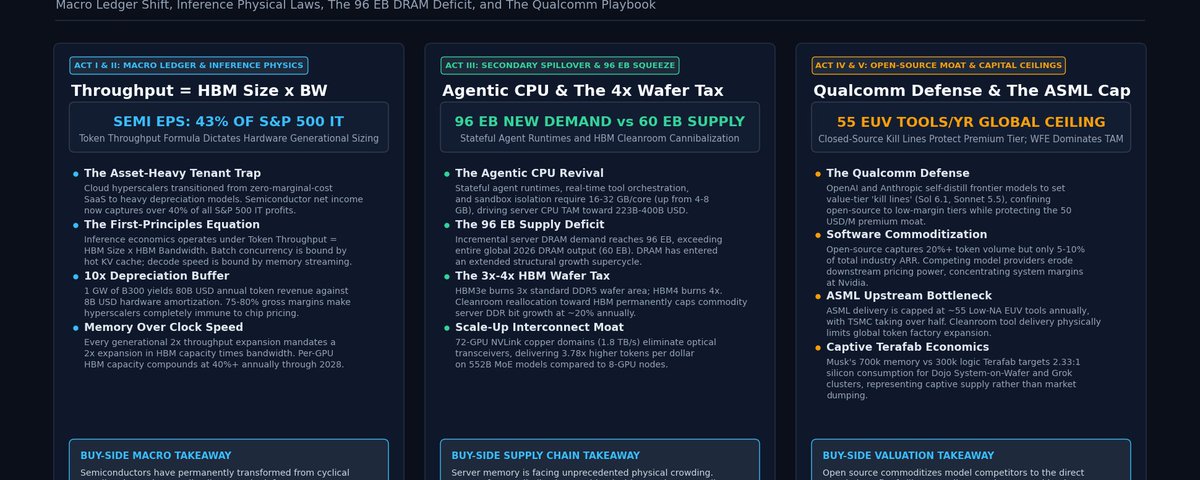
1/5 The Macro Ledger Shift: 2026 completed the permanent transition of computing capital allocation.
Semiconductor net income expanded to 43% of all S&P 500 IT profits (up from <20% in 2023).
Cloud hyperscalers transitioned from zero-marginal-cost software distribution into asset-heavy tenants. Infrastructure CapEx now consumes 35% to 42% of operating cash flow, turning physical silicon into the primary rent collector of technology.

4/5 The Gigawatt Ledger & The Qualcomm Defense: Open-source model price deflation failed to dent hardware CapEx.
1 GW of B300 hardware generates ~$80B in annual token revenue against ~$8B in annual 6-year hardware depreciation. Revenue runs at 10x hardware amortization.
OpenAI and Anthropic executed the Qualcomm playbook: self-distilling frontier models into cost-efficient 'kill lines' (Sol 6.1, Sonnet 5.5) that confine open source to low-margin value tiers.
5/5 Supply-Side Physics: Physical equipment delivery sets the global token ceiling through 2030.
ASML tool output is capped at ~55 Low-NA EUV scanners annually, with TSMC consuming over half for 2nm/A16 logic. Memory cleanrooms cannot expand fast enough to match 40%+ per-accelerator HBM CAGR.
Captive projects like Musk's Terafab (700k memory / 300k logic) reflect advanced packaging's 2.33:1 silicon consumption ratio for internal SoW clusters.
Nikkei reporting Elon Musk targeting 1M WPM for Terafab by 2032 (700k memory / 300k logic) validates the hardware physics of AI token factories.
Silicon Ratio: The 2.33:1 memory-to-logic split directly mirrors advanced packaging wafer consumption, where one compute wafer requires 3x to 4x its area in stacked HBM dies.
Captive Consumption: This represents captive supply for Dojo System-on-Wafer and Grok clusters, insulating internal roadmaps from merchant HBM allocations.
Equipment Multiplier: Building 1M WPM requires $150B+ in cumulative tool CapEx, acting as a massive structural tailwind for WFE leaders ($ASML, $AMAT, $LRCX).
The core hurdle is mastering 1c/1d DRAM yield stacking and securing EUV tool slots in an already rationed global supply chain.
1/5 Token economics in the generative AI era operates under a governing physical formula:
Token Throughput = HBM Size x HBM Bandwidth
Batch size is bounded by hot KV cache capacity in HBM, which scales linearly with concurrent requests. Decode speed per user is bounded by HBM streaming bandwidth.
To double generational token throughput from Blackwell to Rubin, HBM Size x Bandwidth must double. Per-GPU HBM capacity compounds at 40%+ annually through 2028. Hardware throughput is tethered to memory roadmaps.

4/5 Single-gigawatt cluster unit economics show why hyperscalers absorb hardware price hikes:
1 GW of B300 hardware generates ~$80B in annual token revenue. Amortized over a 6-year operational lifecycle, annual hardware CapEx is ~$8B.
Revenue runs at 10x hardware depreciation, supporting 75% to 80% gross margins on flagship token serving. NeoCloud clusters command $40B to $50B/GW annual rental run-rates.
Hardware price increases are readily absorbed because gross margins provide an eight-to-ten-fold cash flow cushion.
5/5 Open-source commoditization follows the historical semiconductor playbook:
OpenAI and Anthropic execute the Qualcomm strategy: self-distill frontier models into cost-efficient 'kill lines' (Sol 6.1, Sonnet 5.5) that confine open-source models to the low-margin value tier.
Open-source weights capture >20% of token volume but only 5% to 10% of total industry ARR, leaving the $50/M premium tier intact.
Software layer commoditization benefits Nvidia ($NVDA ) directly: multiple competing model providers erode customer pricing power, concentrating system margins at the physical silicon layer.
“.. I was unfaithful to my wife,” he said. “My actions hurt her and our children. There is no excuse for what I did.”

Jensen has walked a geopolitical tightrope for three years: lobbying Washington as America's AI champion while engineering compliant silicon (H20) to maintain China revenue.
The transmission mechanisms are severe:
Key-Man Discount: Jensen embodies $NVDA's technical and commercial moat. Subpoenas or security clearance reviews introduce leadership overhang at 30x+ P/E.
BIS Regulatory Ratchet: Political heat closes remaining export loopholes, liquidating residual China datacenter revenue.
Hyperscaler Diversification: Cloud giants actively seeking to curb Nvidia's 75% gross margins gain political cover to accelerate proprietary ASICs (Google TPU, AWS Trainium).
Regulatory shifts reshape capital allocation across the AI hardware stack.

The classic Pareto frontier trap in inference marketing.
AMD ($AMD) MI355X hitting 1330 tok/s/user via TileRT is a batch-1 speed run that drives hardware utilization into the floor. The TileRT dot sits right at zero tokens per dollar.
When serving DeepSeek 552B at scale, GB300 NVL72 ($NVDA) delivers 1.7B tokens/$ versus 0.45B for MI355X: a 3.78x efficiency advantage. Even with MI355X priced at $1.50/chip-hr versus $2.31 for GB300, a 72-GPU NVLink scale-up domain and native FP4 execution crush raw chip-hour discounting every time.


An expert call on Intel ($INTC) revealed the underlying manufacturing and packaging yields driving the Q4 gross margin collapse to 38%:
EMIB assembly yield sits at only 40.5%
Intel allocated roughly $3.5B of next year's capex to EMIB. Substrate yield rose from ~30% in Q2 to a 50% Q4 target, aiming for 60% in Q1 next year. However, overall assembly yield is currently stuck at 40.5%. Scrapping nearly 60% of units during advanced packaging is the direct physical driver of elevated manufacturing write-downs. Capacity targets are 20k units baseline by end-2027 and 80k units by end-2028.
14A faces near-term yield headwinds
Total capex next year is guided between $27B and $33B ($30B median), focused on 18A and 14A nodes. While 18A is ramping steadily, 14A is encountering yield headwinds and near-term capacity constraints. Cost reductions on Panther Lake depend strictly on yield gains and cannot be modeled linearly.
External foundry revenue remains below 2%
Internal product divisions still account for over 98% of foundry revenue. Tesla is in contract negotiations but has not paid a deposit, while Microsoft, Google, and Amazon remain in evaluation phases. Without binding customer prepayments, the $30B annual capex burden sits entirely on Intel's balance sheet.
US manufacturing cost parity
Intel retains structural advantages in large-die, multi-chiplet, and multi-HBM architectures. Given high expat labor and union overhead at TSMC's Arizona fabs, US-based wafer manufacturing costs between the two are moving toward near-parity.
With assembly yields under 50% and external customers yet to write deposit checks, Intel's heavy foundry operating drag will take quarters to clear.
15 years of precedent backs you up: Altera 14nm, LG Nuclun, and Spreadtrum all died in evaluation gear. Intel IDM DNA lacks TSMC standard OIP ecosystem. Porting proprietary Synopsys/Cadence libraries to Intel PDKs costs $100M+ with zero guarantee of volume wafer delivery.
Follow the cash. In 15 years, external customers signed MOUs but wrote zero binding prepayments. Apple pre-funds TSMC cleanrooms; hyperscalers leave Intel with $30B in balance-sheet capex. Until an external tier-1 wires a $1B non-refundable deposit, evaluations are just theater.
Intel 40.5% EMIB yield proves process tuning hit physical limits. Absorbing 6x CTE shear stress between silicon bridges (2.6 ppm) and organic ABF (16 ppm) demands compliant buffer layers.
The persistent defect rate directly validates the strategic pivot to Glass Core.